03 - Controlling Air Gaps Using OrCAD X and Allegro X Tools
The shape of things to come is the dynamic shape. Actually, it’s a well established pattern of using the constraint set to directly affect the outcome. The smart copper “sees” other traces, vias and other shapes that have different nets and works around them. What the shape does with a friendly pin or other feature is part of a parallel set of rules regarding Same_Net properties. The exact amount the shape pulls back is entirely up to the user - you.
As with the line width parameters, the spacing constraint tab has a default set of air-gap parameters. Other rules may be in effect for various reasons around impedance, magnetic coupling, crosstalk or other isolation goals. The numerical value of the air-gap will always be, “It Depends”.
The first dependency is the nature of the two features. You’d certainly do everything you could in the placement phase to avoid routing the receive chain next to an external oscillator. Mind the established aggressors and potential victims to keep them organically separated. It takes some finesse to get everything to play well together. Coexistence is pretty easy when you have all the board space you want. Shrinking down to the form factor unleashes the unknown threats. Do that layout and then, find out.
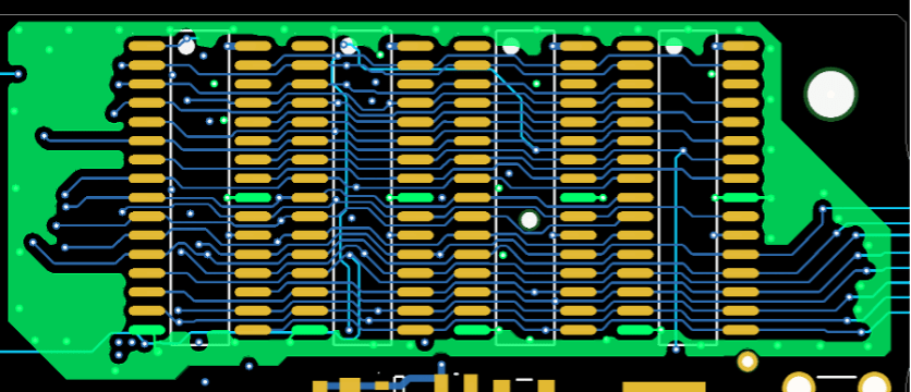
Figure 1. The green shape is a partial ground plane on the outer layer. It is a dynamic shape used to isolate the four memory chips from nearby circuits while forming around the existing circuit pattern. A static shape would be used to create an EMI shield or other polygon that did not dodge around the existing circuit.
Once you’ve found out the hard way, (and by that I mean boards come in and there’s some issues that were not foreseen) there are two concerns, first is correction of the problem and second is prevention of the problem down the road. The correction path involves separating the annoying parts. The prevention path is partly in the realm of the constraint manager. We may add a new constraint set that restricts those unforeseen things from happening again.
High speed and high frequency transmission lines typically require a guard trace or grounded copper flood that is pulled back a specified distance from the transmission lines. At the same time, the walled garden is closing the gap to the ordinary signals beyond. Safety is first which makes performance secondary. High voltage will require sufficient space to prevent arcing. Learning about this part of the tool will make life easier during routing wherever shapes are in the picture.
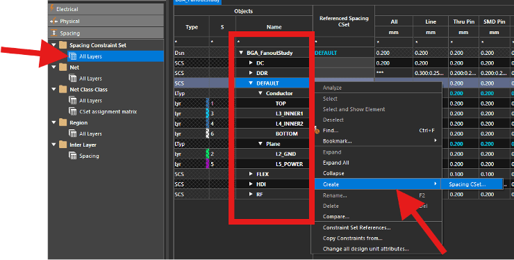
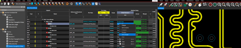
Figure 2. The first page of the Spacing worksheet selector allows the creation of new Spacing Constraint Sets. Right Mouse on the name of an existing constraint set in order to copy it for revisions. Each constraint set will define spacing requirements sorted 11 different ways. The Line values are shown but the Shape values are the definitive ones as far as generating copper pour. Each attribute (Lines, Pins, Vias, etc.) has its own tab that interacts with the others. This helps with management of the air gaps all around us.
Intra-Pair Spacing
It’s not uncommon to express the air-gap as a function of line width. The typical air-gap between controlled impedance traces will often be three times the line width or five times if you want to be conservative. It’s not really the line width that matters as much as the distance in the Z-axis to the reference plane. Given a typical dielectric constant, the line width and the dielectric thickness are fairly close in value. The width of the line stands in as a shorthand for this rule of thumb.
The practical effect of the rule is that we don’t want long runs of parallelism when we’re routing a bus. The grain of salt to take from this rule is that there are going to be times when the design rules cannot be met due to spacing limitations around fine pitch devices.
Inter-Pair Spacing
Differential pairs have a gap between the positive and negative members; the interpair gap. Here, it’s a matter of whether the pair is closely or loosely coupled. Closely coupled differential pairs have a gap that is equal to or less than their line width. Conversely, loosely coupled pairs have an air-gap that is greater than the trace width by some measure.
On one hand, the tightly coupled diff-pair will use less space and excel at rejecting common mode noise. In addition, the bends have minimal effect on skew between the positive and negative connections which should make phase matching possible with less uncoupled length.
When the fab shop wants to make an impedance adjustment to differential pairs, they are most likely to change the width of the lines which also changes the gap. They are working with what you’ve given them in terms of the pitch of the two traces. Their line width updates are usually pretty small but the air gap changes along with the line width. Their options are limited but they always seem to figure it out in the DFM cycle.
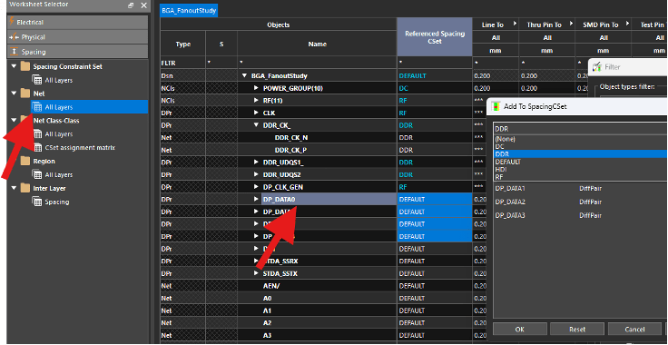
Figure 3. The second tab down on the Spacing worksheet is labeled “Net/All Layers”. This is where the rules created in the first spacing tab are applied to groups, pairs and individual nets. The spacing values presented in the Nets tab impact all layers rather than the layer-by-layer approach in the Spacing Constraint Set. If the numbers are replaced by the three asterisk trio, it means that different values are in effect for the various layers while a number there means that all spacing values are the same for that item.
Can You Give Me Some Space?
Meanwhile, loosely coupled pairs present a challenge of their own. The ideal geometry can be difficult to implement on fine pitch BGA devices. There may be a transition area where you work your way out of a congested pin field. Being the opposite of tightly coupled, the trace that takes the outside of a bend goes considerably further than the one with the inside route.
The disparity works against what it means to be differential and suggests that we do a phase tune for every bend that isn’t immediately countered by a bend in the other direction. We could ignore a short S-turn but would compensate for an isolated 90 degree bend when using loosely coupled differential pairs. The goal is to have two signals making their way down the conductors at the exact same instant. Any transient conditions along the way should affect both signals so that it all cancels out. It sounds simple but things are happening really fast.
… the higher of the two (spacing) values apply when traces with different spacing rules meet
This technology is favored among the graphics set. It’s a common request when doing MIPI and HDMI or other graphics pipelines. A quick look at application notes from NXP regarding display port recommends 5 mil lines separated by 7 mils. One lane of two tracks adds up to 17 mils plus the personal space that a diff-pair wants adds 15 mils per side so 47 mils (1.2 mm) total. Fortunately, the spacing rule does not stack so only the higher of the two values apply when traces with different spacing rules meet, not the total.

Figure 4. The Net Class-Class tab is where priorities can be set. As usual, the Objects columns named Type, S, and Name are where the filter can be invoked with a right mouse-click. Creating or managing Net Class membership is started with a right mouse-click on the net or class names in the Name column. In this case, the POWER GROUP is up for editing.
My first exposure to the differential pairs was on an edge router. These are big enterprise boards that carry the data from the main internet connection to users throughout the office. I did two of these things on a six-month contract. On the outside, it’s a box with a row of ethernet ports across the front panel. On the inside, it had four individual processors, a memory controller and a row of expansion slots after the solder-down memory.
One part of the 12-layer board was set aside for the power supply. The power supply is normally a separate thing since it runs hot. It’s also one of the most likely failure points once everything has settled into the bathtub curve for reliability. The rest of the board was separated from the power supply with a wide route keep-out zone that covered the ten internal layers and parts of the outer layers.
That wasn’t my idea. There was a man in Rochester NY who was a Regulatory Engineer. He was managing the power supply from 110/120VAC in to 5VDC out. He had width and air gap provisions for every node. A big transformer or inductor (make a fist!) connects to a thumb-sized resistor. It was tricky bringing the two leads together without breaking the rules for the transformer and inductor.
Trace width was used to define the copper, but shapes and keep-outs were used for the actual connections. Of course, it was static copper that did not yield to outside influence. Satisfying that guy (who left every day at noon!) was a pain but I came out of it able to control the copper to his liking. He basically wanted proof that it could not be designed any other way than what was stipulated. I’ve used those lessons over and over for design verification.
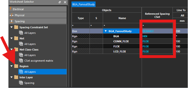
Figure 5. Selecting the appropriate rules for a region happens as you create the shape. Defining what that means in terms of spacing falls on the selections seen here and made in the Referenced Spacing Cset of the Region tab of the Spacing Constraint Set worksheet.
It’s hard to overstate the importance of getting the right amount of space for each situation. Prior to fabrication, the entire panel is a solid sheet of copper. The process in the factory is to etch away the parts we don’t need. What we’re creating in the factory is the air-gaps more than the metal. If we’re doing an additive process, well then the air gaps still matter. The numbers may shrink so we’ll be even more vigilant in that case.
Using -1 as a Value in the Spacing Table
I’ll share another constraint quirk that you might find useful. Have you ever created a wirebond cage? One of the flukes of wirebonding is that the wire flies over the top of the board with nothing but air for dielectric. The rule for 1 mil wire is a 1 mil gap. The inboard wire can fly right over the pad of the outboard wire shorting to the pad for the wire.
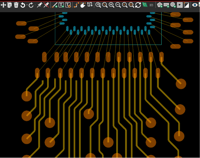
Figure 6. Connecting the die (Blue) to the board or substrate (Brown) with wirebonds can be done with a one mil air gap from wire to wire. Note how the wires are on the etch layer so we can apply this one mil trace/space rule around the wirebond cage. An exception to the rule where the wires to the outer row pass over the pads for the inner row. That’s where the negative one value for via to line allows the wirebond. Once that is done, the wire can be represented in an assembly detail. Then, the etch layer is available to finish the last segments to the inner row. The rules then go back to normal by deactivating the constraint region around the wirebond cage.
First, create a region around the passivation openings (where the wirebond starts) and set the Etch to Pin spacing value to -1. When the spacing rule equals negative one, the wire will cross over the pad with no design rule violation. The other air gaps like the 1 mil wire-to-wire rule remain in effect. You would memorialize the wirebond solution with a fab detail.
The 1 mil lines representing the bond wire would be removed from the etch layer so that the fan-out can be completed on that layer. I use Layer 1 to “route” bond wires for the line lock so that the 45 degree maximum launch angle is locked in. Further, the wire length should not exceed 100 times the diameter so a max length could be enforced as well. We will get to that next. You can really go deep with constraint regions inside of constraint regions as you work from the chip to the wirebond cage to the outer areas of the board or substrate.
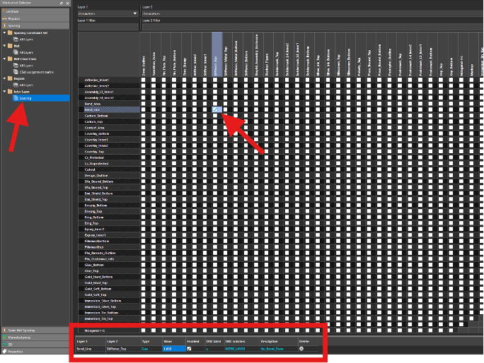
Figure 7. The Inter Layer Spacing window is almost too big for my 5K monitor. This is a sprawling check box field where I’m currently selecting the square to add a rule between the Stiffener_Top layer and the Bend_Line layer. I chose to add a gap of 1. 6 mm. There is a separate window from this one focused on managing metal layers.
So, that’s all I have space for today. This is likely the first design rule you’re going to want to solve in most cases. The spacing rules take time to grow into your flow. The standard rule set may be all you need. Get ready for the next dimension. The 4th dimension. The Electrical Constraint Set and how the timing budget on the PCB affects the system level performance. Part Four awaits.
View the next document: 04 - PCB Constraints: Controlling Trace Length For Digital Circuits Using OrCAD X and Allegro X Tools
If you have any questions or comments about the OrCAD X platform, click on the link below.
Contact UsClick here to download the PDF.