Interstitial Vias and How Using Them Can Help Your PCB Design
Most PCB designs benefit from the use of vias for grounding by tying copper flood on various layers together. This helps to prevent stray current from building up on a copper plane. These ground vias will need to be spaced close enough to prevent excessive undesirable radiation while being spaced far enough apart to prevent the board from breaking like a saltine cracker or blocking any other routes from passing through on other layers. The interstitial via is a way of getting the best of both worlds.
The fanatical effort you give to protecting the receive chain will be reflected in the difference between your design and the others who use the same chip set.
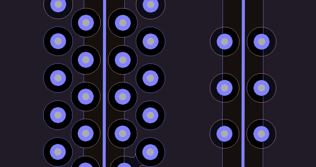
Image credit: Author. Leaving a web of copper allows traces to slip past on other routing layers.
Background
A path between ground planes becomes super-important when a high-speed digital or any sort of RF transmission line has to transition from one layer of the board to another. The currents generated by those traces will radiate and, if unchecked, will likely fail when it comes to emissions testing for regulatory compliance. The via, being an unavoidable impedance discontinuity, presents one of the worst areas for electromagnetic radiation. A gap in the ground plane below the trace would also be an emissions problem of similar magnitude.
The Federal Communications Commission establishes two main criteria that, taken together, provide for coexistence. The first principle is that your device must not interfere with the workings of other devices. On the other hand, the product your company puts on the market should have a reasonable tolerance for whatever noise is present. They say that good fences make for good neighbors. A quiet device that is immune to the workings of nearby devices is the one that will pass and be allowed to compete in the market.

Image Credit: Design Idea - A permeable perimeter is fine if you have a lot of space as a buffer.
Check the Data Sheet
A good component vendor will provide some guidance on what it takes to succeed with their product. That information can take the form of application notes on the datasheet or a so-called “reference design” that incorporates the best practices. I recall a particular Chromebook that used the Intel Skylake device. Before diving in, they gave me an 800-page volume and that was only for the physical end. The Software team had one of their own. The first 200 or so pages of that thing could be used as a general best practices of PCB design. Every conceivable memory configuration took up the middle of the work. Then, details about each pin followed.
Chip vendors want you to succeed so that the orders keep coming in. That is their incentive to craft a conservative approach to the board that will enable their part to perform at its best in most conditions. When I was doing a design for the Qualcomm Snapdragon 845 that is being used in current (2019) flagship phones, one of the specifications involved an isolation requirement of 100dB! In the macro-world, that would be like putting up a roof on a house such that a commercial jetliner could take off right overhead and you wouldn’t miss a line from your favorite TV show.

Image Credit: Lowes - Nothing to see here although airflow (and routing) will not be blocked.
Going Analog
The fresher RF expert asked me what the minimum spacing for micro-vias would be. I let on that we could position them such that one capture pad was tangent to the other. Little did I realize that the intention was to line all of the radio transmission lines with vias at a pitch equal to the capture pad size.
Even with that zero-gap, the simulations looked a bit scary. This was not going to be a PC board in a phone-sized form factor but we were setting up the radios as if they were. We needed to get a leg up on that part as coexistence became the long tent-pole of the design. You might be surprised at just how many radio-type devices and modules go into a phone. We had to protect each circuit from all of the others. It was a via slam inside the shielded areas and a double row in interstitial vias on the runs from the Snapdragon to the various wireless devices. Of course, it took two more years of iterating before the circuit passed muster in the actual form factor. Going into the phone business is a serious commitment.
Correct By Design
One way of ensuring that priority is given to this notion is to establish the copper flood and subsequent ground via locations as early as possible. Place the RF chains, pour copper, populate the vias. Then work around those elements as you complete the not-so-critical placement and routing pieces of the puzzle. It is so much easier to do this part earlier than to try to shoehorn the compliance into the project at the end of the layout process.
While your design may not require 100 dB isolation, having a tight Faraday cage around the most vulnerable circuit can’t hurt. Caging up the most aggressive lines is the flip side of that coin. Passing FCC with margin to spare makes you a hero. If your design has room, it makes sense to take the nearly free performance upgrade that the interstitial via offers.
Granted, this takes up precious space. Take the space from day one then relocate a via where the design mandates their removal. Fight for those vias! The fanatical effort you give to protecting the receive chain (or the antenna) will be reflected in the difference between your design and the other players who use the same chipset. There are other differentiators that come at various price points. This is the money.