Can You Afford to Skip the CAM Process When You Tape Out a Printed Circuit Board?
Computer Aided Manufacturing (CAM) is a profession that lies between the buyers' data and the seller’s process.
You may have seen the advertising already. Some PCB fab shops will provide a quotation based on a questionnaire that details the pertinent factors; starting with stack-up and finishing with a list of extra options. As you go through the order form, the default values are the no-cost-adder options. But wandering in the wrong direction with, for instance, the minimum air gap will incur a mark-up over the unbelievably low price for an order of printed circuit boards. One of those options is a going over by the vendor’s CAM department to prep your data for fabrication.
Your data obviously passes your CAD program’s design rule checks for shorts and opens. Your soldermask layer may be expanded in a way that avoids slivers between pads. All of the ink is pulled back from those mask openings as well. If the board is that well designed and wide open enough for all of the tolerance anyone would need for a simple circuit, take your chances. There are still things the CAM operator can do for you. The question is, “Do you need it?” In almost every case, I would say yes.

Image credit: Siemens
It is hard to find a PCB design that doesn’t have some form of controlled impedance. That, alone, would trigger a review. PCB fabrication often involves a pre-distortion of the data. Known as etch compensation, the fabricator’s front-end team will globally widen or narrow all of the artwork geometry so that when everything is said and done, the PCB comes out with etching that best matches the design intent. Adding or taking away even one one-thousandths of an inch can tank an impedance requirement.
There winds up being a lot of hard edges to a circuit. The fact is that the etching process is more organic than laser sharp. The fab shop adds a photoresist layer or mask over the board before the whole thing goes into a tank of acid for a precise amount of time. This is enough to dissolve the unwanted copper without severely undercutting the mask. The actual time in the bath depends on the starting and ending copper thickness; it’s not a constant.
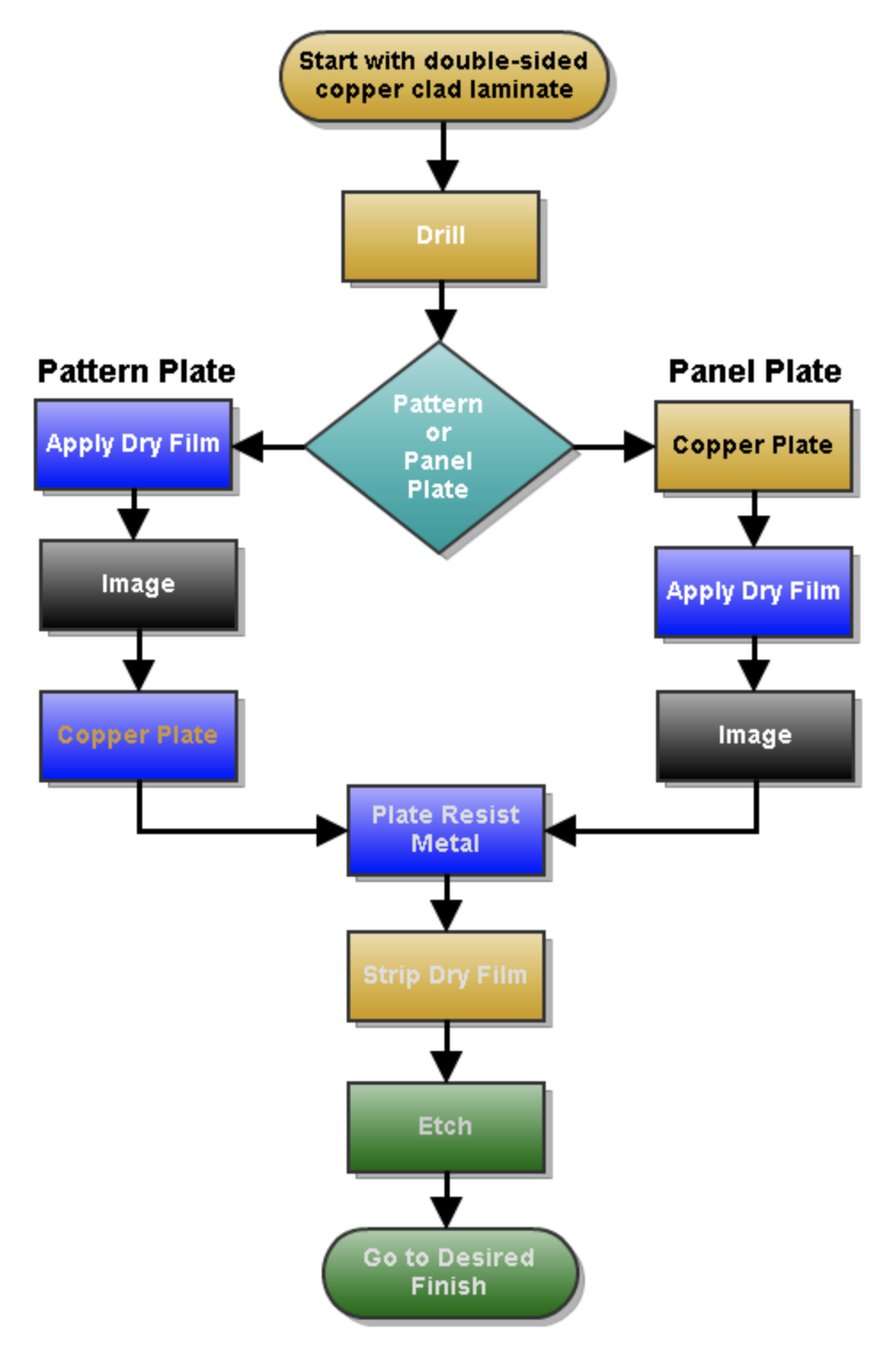
Image credit: Wiki Commons
Then they get it out of one tank and immediately into another tank that washes out the metal eating chemical. A tiny bit of the acid stays in the tight corners and continues to fester away to over-etch that spot leaving the board with a possible open connection. Before that can happen, the CAM operator can smooth those acute corners out, especially around the junction from a via to a line or pad. Though common on flexible circuits, not many board designers are inclined to add a fillet to all of the via and pad junctions. Taken together, etch compensation of smoothing the jagged edges are where the CAM benefit the copper layers the most.
If you have seen a flow chart of the way a PCB is fabricated, you would see that there are a number of steps that use a derivative of the artwork provided by the customer. Global micro-edits are a tool used to enhance the final outcome. In moments of candor, I’ve heard that the edits can be rather extensive for a challenging design. I would be shocked if I knew the full extent of their edits, or so I was told.
Non-metal layers are easier to overlook when the struggle with the connections are in full swing. Come to the end-game and the design improvements that seem to come out of the woodwork keep the metal layers front and center. The time-crunch that comes with the release process increases the chances of an incidental error on the silkscreen. If you are comfortable with skipping the CAM step and can live without any fancy technology, there is the option of quick turn without any of the back-and-forth with the fab shop.
Image source: Sun Circuits
There are quite a few restrictions for using the automated service. My hypothetical PCB order was as follows:
-
Two-inch by two-inch size.
-
20 pieces.
-
4 layer .062” thickness.
-
One week turn.
With no other selections beyond the defaults, the price for that order comes to $478 or a unit cost of $23 per board. The cost of NRE (Non-Recurring Engineering) for the sanity check added $280 and raised the unit cost to $35 and change, or about double the cost; close to $900 for the order. Compare that with the upcharge from tin/lead finish to a more sensible ENIG finish which will push the individual cost from $23 to $34 without the one-time charge.
Clicking those two boxes bring the total for 20 boards to approximately $1200 US Dollars. The other parameters include larger vias and wider lines than I’d usually use. Each additional detail drives cost and the quote up instantaneously taking all factors into consideration. Poking around the quote generator gives a good idea of what a full-service job should cost. If you can live with six mil traces and fifteen mil finished hole sizes, along with a list of other parameters, you might be able to cut some cost and schedule corners.
Hobbyists and experimenters can probably get by with a simple enough design. If failure is not an option or you require some higher technology with your build, I would stick with a human interface and a professional Computer Aided Manufacturer instead of just the computer.