Constraint Driven Design in OrCAD X
Key Takeaways
-
Constraint driven design standardizes PCB development by enforcing predefined electrical, physical, and manufacturing rules throughout the design process.
-
Real-time design rule checks (DRC) and cross-probing between schematics and layouts help engineers catch errors early and enforce design requirements automatically.
-
Reusable constraint templates streamline multi-board and iterative designs, ensuring consistency across different projects while saving time on setup and verification.
Constraint driven design is a methodology that embeds the rules and requirements of a PCB directly into the design process. By defining and enforcing constraints upfront, engineers can ensure that performance, manufacturability, and reliability requirements are met from the outset.
This article explores the fundamentals of constraint driven design, and then delves into how OrCAD X enables this approach through its advanced Constraint Manager.
Constraint Driven Design in OrCAD X
Constraint driven design in OrCAD X integrates predefined electrical, physical, spacing, manufacturing, and 3D rules directly into the PCB design process. This approach, along with the layer-dependent nature of PCB layouts and the need for dynamic adjustments during design iterations, makes constraint management a critical element in creating robust, manufacturable circuits.
OrCAD X streamlines constraint management by synchronizing rule definitions between schematic capture and layout. The tool automatically enforces design rules that you set, allowing you to focus on fine-tuning your design for optimal performance. With capabilities like real-time design rule checks (DRC), cross-probing between schematics and layouts, and reusable constraint templates, OrCAD X minimizes errors and enhances consistency, allowing rules to flow effortlessly throughout the design process.
Types of Design Constraints
|
Type |
Scope |
Applicationvs |
|
Electrical Constraints |
Focuses on achieving optimal electrical performance by maintaining signal integrity, precise timing, and efficient power distribution. Also includes high-speed design constraints with length matching, skew tolerance, and via stitching. |
|
|
Physical Constraints |
Control the board’s layout and manufacturability, ensuring effective component placement and proper geometric configurations. |
|
|
Spacing Constraints |
Ensures proper clearances and separations to prevent shorts, minimize EMI, and maintain mechanical and thermal reliability. |
|
|
Manufacturing Constraints |
Aligns design parameters with fabrication capabilities to reduce errors, enhance yield, and lower production costs. |
|
|
Constraint Regions |
Enables localized rule application by overriding global constraints in specific, complex, or dense board areas. |
|
Design Constraints in OrCAD X
OrCAD X utilizes Net Classes, Net Groups, and Regions to efficiently organize and manage design rules. These features allow for a structured, verifiable, repeatable, and specific application of constraints, ensuring consistency across the design.
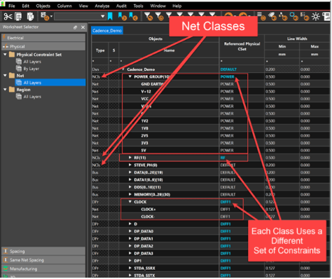
Screenshot of Constraint Manager displaying parent-child relationship in terms of net classes with their rules applied
Net Classes, Net Groups, and Regions
-
Net Classes: Nets that share similar characteristics (e.g., all power nets or all high-speed signals) so that physical constraint sets (CSet) like trace width or via rules can be applied collectively.
-
Net Groups: For broader organization across multiple domains, use net groups to manage collections of nets with common functional requirements. Spacing Constraint Sets (SCS) can be defined for these groups to ensure consistent clearances.
-
Regions: In areas with specialized requirements—such as fine-pitch BGA zones or dense DDR memory areas—regions are created to apply localized constraint sets that override the global rules. This allows for tighter control in critical areas without impacting the entire board.
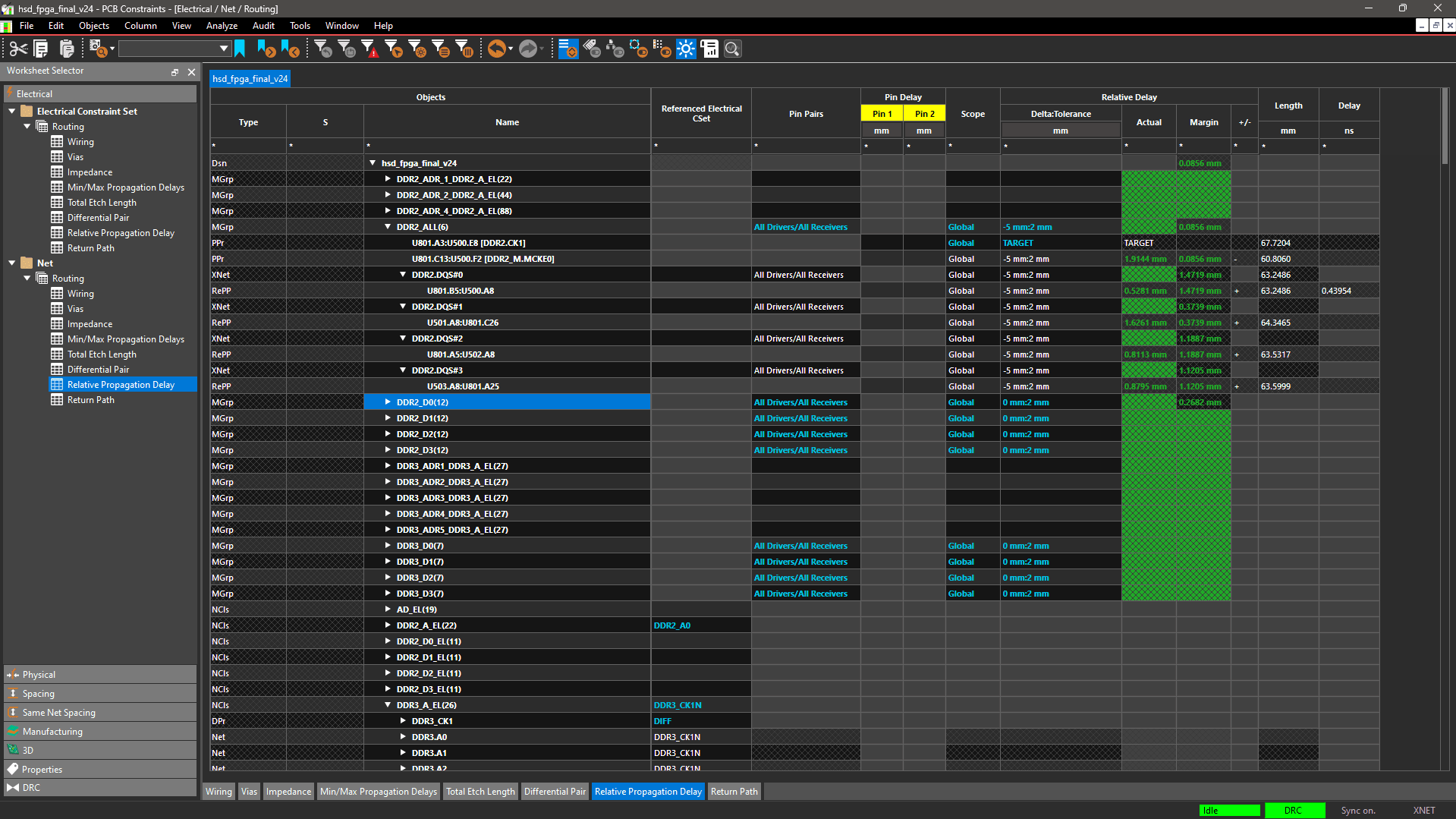
Example: Constraint Driven Design for DDR Memory
A comprehensive DDR memory design must address both electrical and physical challenges to meet stringent high-speed performance requirements.
Electrical Constraint and Timing
-
Setup and Hold Time: DDR memory transfers data on both rising and falling clock edges, doubling throughput while tightening the timing window. Each data line must meet strict setup and hold time requirements, defined by the clock (CLK) signals that establish when data must stabilize. Use serpentine routing to deliberately lengthen traces and introduce precise delays, ensuring that data signals stabilize within the required setup and hold windows.
-
Differential Pair Matching and Impedance Control: DDR designs typically use differential signaling to reduce noise and improve signal integrity. Equal trace lengths for differential pairs minimize skew and balance propagation delays. Consistent impedance matching helps reduce reflections and crosstalk. In OrCAD X, you can set rules to enforce equal trace lengths for paired signals and define the characteristic impedance for both single-ended and differential pairs.
-
Power Integrity and Termination: Reliable DDR operation requires clean supply voltages and stable reference levels. Proper termination of address/command lines minimizes signal reflections, while controlled impedance traces and bypass capacitors help maintain voltage stability. Configure termination schemes by specifying resistor values and routing guidelines, ensuring bypass capacitors are strategically placed near termination points.
High-Speed Design Constraints
High-speed design constraints are essential for maintaining signal integrity in high-frequency circuits. Key considerations include controlled impedance, length matching for differential pairs, via stitching for return paths, and signal rise time management.
-
Topology Selection: The routing methodology plays a pivotal role in DDR design. While T-Topology was previously used in DDR2 designs, modern DDR3 and DDR4 systems benefit from Fly-By Topology. This daisy-chain approach minimizes trace stubs and provides better signal integrity by reducing impedance discontinuities.
-
Layer-Dependent Routing: Routing on inner layers (stripline) versus outer layers (microstrip) results in different signal characteristics. High-Speed Design Constraints account for these variations, ensuring that the overall time-of-flight (TOF)—which includes both the PCB trace length and any additional lengths inside component packages—is precisely controlled.
By leveraging OrCAD X integrated constraint management tools, designers can enforce these technical specifications from the schematic capture phase through layout, ensuring that every DDR interface is robust, reliable, and manufacturable.
Physical and Spacing Constraints
-
Trace Length Matching: Precise trace length matching is critical for maintaining synchronous data capture across DDR signal groups, such as CLK-to-Address/Command (CLK/ADDR/CMD), CLK-to-Strobe (CLK/STB), and Strobe-to-Data (STB/Data). This ensures that propagation delays remain within manufacturer-specified tolerances. In the CM, you can set maximum tolerances for trace lengths.
-
Component Placement and Routing Clearances: Optimal placement of DDR memory chips, controllers, and supporting circuitry minimizes signal path lengths, reduces interference, and contributes to overall signal integrity. Organize signals using Net Classes and create a Physical Constraint Set (CSet) to define rules for trace widths and via specifications. Adequate spacing between high-speed DDR traces is vital to prevent electrical shorts, minimize electromagnetic interference (EMI), and maintain consistent impedance.
Constraint driven design is crucial to ensure your board is reliable and manufacturable. With OrCAD X, engineers can easily create and manage electrical, physical, and spacing rules using the robust Constraint Manager. Explore how Cadence's PCB Design and Analysis Software and OrCAD X platform streamline constraint setup and ensure reliable PCB performance.
Leading electronics providers rely on Cadence products to optimize power, space, and energy needs for a wide variety of market applications. To learn more about our innovative solutions, talk to our team of experts or subscribe to our YouTube channel.