Design Rule Check Using OrCAD X
Key Takeaways
-
OrCAD X performs real-time and batch Design Rule Checks (DRC) to detect violations in trace widths, spacing, vias, and component placements before fabrication.
-
Electrical Rule Checks (ERC) in OrCAD X identify connectivity issues like short circuits and floating nodes, ensuring electrical integrity alongside physical design compliance.
-
OrCAD X provides visual DRC and ERC error identification with interactive debugging tools, allowing designers to efficiently resolve violations and optimize PCB layouts.
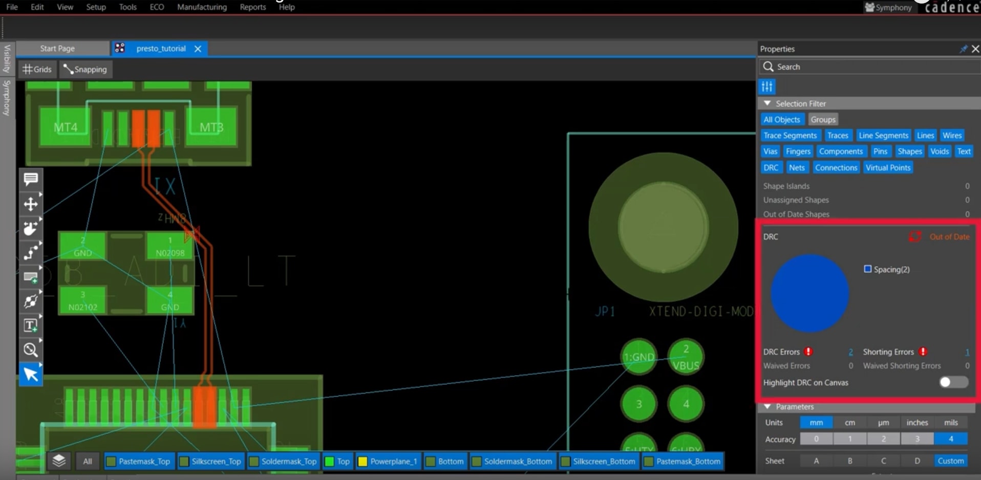
DRC flag on OrCAD X Presto canvas with further detail in the pie chart.
A Design Rule Check (DRC) is a critical verification process in printed circuit board (PCB) and integrated circuit (IC) design that ensures a layout complies with manufacturing and performance constraints. By analyzing key design parameters such as trace widths, clearances, via sizes, and component placements, DRC helps eliminate costly errors that could lead to defective products or manufacturing inefficiencies.
In OrCAD X, design rule checks can be performed at multiple stages of the PCB design process, including schematic capture and PCB layout. These rules include constraints on trace-to-trace spacing, minimum feature sizes, copper-to-board edge distances, and via tolerances.
During the schematic capture phase, DRC ensures that the electrical design follows defined constraints and uses Electrical Rule Checks (ERC) to verify the electrical integrity of a design, reducing the risk of incorrect net connections or voltage mismatches. Once the layout is completed, physical DRC checks validate critical parameters such as trace width, spacing, and via configurations.
Advantages of Using OrCAD X for Design Rule Checks
|
Advantage |
Reasoning |
|
Automated and Real-Time DRC |
Enables immediate identification and correction of design rule violations. |
|
Configurable Constraints |
Allows designers to define and modify constraints based on project requirements. |
|
Error Visualization |
Highlights rule violations directly in the PCB layout, making debugging more efficient. |
|
Enhanced Manufacturability |
Reduces the risk of PCB fabrication and assembly defects by enforcing industry-standard constraints. |
Design Rule Check in OrCAD X
OrCAD X provides an extensive set of DRC capabilities to ensure that PCB layouts comply with manufacturing constraints and industry standards.
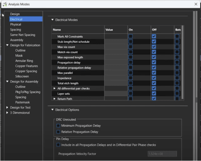
OrCAD X Constraint Manager Window Showcasing Possible Electrical Rule Checks
Design Rule Check Features in OrCAD X
OrCAD X offers both online and batch DRC, enabling real-time feedback during design as well as comprehensive error reporting for final verification. The tool includes the following interactive features:
|
Category |
Constraint |
Description |
|
Spacing Constraints |
Via-to-Via Spacing |
Ensures a minimum allowable spacing between vias to prevent short circuits and improve signal integrity. |
|
|
Net Spacing Types |
Defines spacing rules for different net categories, such as high-speed or power nets. |
|
|
Copper Spacing Constraints |
Enforces rules for spacing between copper features to maintain manufacturability. |
|
|
Etch Text to Copper Shapes |
Verifies spacing between etched text and copper shapes. |
|
|
Package-to-Package Spacing |
Ensures proper separation between different component packages to avoid assembly issues. |
|
Line Width Constraints |
Minimum Line Width |
Specifies the smallest allowable trace width to ensure proper current-carrying capacity. |
|
|
Maximum Line Width |
Limits trace width to maintain controlled impedance and avoid excessive copper usage. |
|
Stacked Vias |
Controls the placement and configuration of stacked vias to maintain structural integrity. |
|
|
|
Via List Constraints |
Specifies allowed via types based on manufacturing capabilities. |
|
|
Via Under Component |
Prevents vias from being placed under critical components where they may cause soldering issues. |
|
Net Constraints |
Net Physical Types |
Defines physical properties for different net classes. |
|
|
Differential Pair Constraints |
Enforces matching rules for differential pairs to maintain signal integrity. |
|
Annular Ring Constraints |
Annular Ring Dimensions |
Specifies the minimum and maximum allowable ring dimensions to ensure via reliability. |
|
Component Placement and Lead Checks |
Through-Hole Pins Under SMD Components |
Ensures through-hole pins do not interfere with SMD placements. |
|
|
Component Lead Checks |
Verifies compliance with component lead requirements. |
|
Fiducial and Outline Constraints |
Fiducial Checks |
Ensures proper fiducial placements for accurate assembly alignment. |
|
|
Outline Constraints |
Defines constraints related to board and component outlines. |
|
Cutout Constraints |
Cutout Constraints |
Controls the placement and size of design cutouts to prevent structural weaknesses. |
|
Design for Manufacturing Constraints |
Design for Assembly Constraints |
Ensures spacing and placement rules for optimal assembly. |
|
|
Design for Fabrication Constraints |
Verifies manufacturability against fabrication limits. |
|
|
Design for Test Constraints |
Ensures accessibility and placement of test points for debugging. |
Finding Design Rule Check Errors in OrCAD X
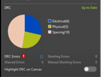
OrCAD X Presto PCB Editor will give you an indication of your design’s DRC status within the properties panel. The DRC errors can be found by clicking on the hyperlink, while an overview of the errors and their types are presented in the pie chart. If you click on a section of the chart, it will then focus on the errors of the given type:
Spacing Errors
Spacing errors occur when traces or other design elements are placed too close together, violating predefined spacing constraints. By selecting the spacing portion of the pie chart, the search panel will automatically open to display all detected spacing errors. Users can further refine the view by selecting specific types of spacing violations. For example:
-
Line to Line Violations: These errors indicate that traces are placed too close to each other, failing to meet the required spacing constraints. To fix them, users can enter Slide Mode, attach a trace to the cursor, and reposition it to increase spacing. The system will highlight any remaining violations with a red DRC marker. Once adjustments are complete and constraints are satisfied, the error is removed from the search panel.
Physical Errors
Physical errors are related to constraints on individual trace dimensions and their layout properties. Upon selecting Physical in the DRC pie chart, the system updates to show specific types of physical violations. A common example is:
-
Minimum Neck Width Violations: These occur when a trace becomes too narrow at a particular point, violating the minimum width constraint. To correct this, users can select the affected trace in the PCB canvas and adjust its width in the Properties Panel (e.g., increasing it to 15 mils). Once the trace width meets the required specification, the violation is resolved, and the error is removed from the search panel.
Electrical Errors
Electrical errors involve violations of signal integrity and differential pair constraints. Selecting Electrical in the DRC pie chart reveals sub-categories such as:
-
Differential Pair Maximum Uncoupled Length: This error occurs when the separation between traces in a differential pair exceeds the allowed length, which can degrade signal integrity. Users can filter the search panel to locate these violations and correct them by adjusting the traces to bring them closer together.
-
Differential Pair Phase Tolerance Violations: These errors indicate that the length of differential pair traces is mismatched beyond the allowed phase tolerance. To fix this, users need to adjust the trace routing to ensure both traces are of equal length. Filtering options in the search panel allow users to isolate and address this specific violation efficiently.
Ensure your PCB layout meets manufacturing and performance standards with a design rule check in OrCAD X. By leveraging the powerful DRC and ERC tools, designers can detect and correct violations in trace widths, spacing, and electrical integrity before fabrication. Explore how OrCAD X and Cadence’s PCB Design and Analysis Software can help streamline your design process and improve product reliability.
Leading electronics providers rely on Cadence products to optimize power, space, and energy needs for a wide variety of market applications. To learn more about our innovative solutions, talk to our team of experts or subscribe to our YouTube channel.