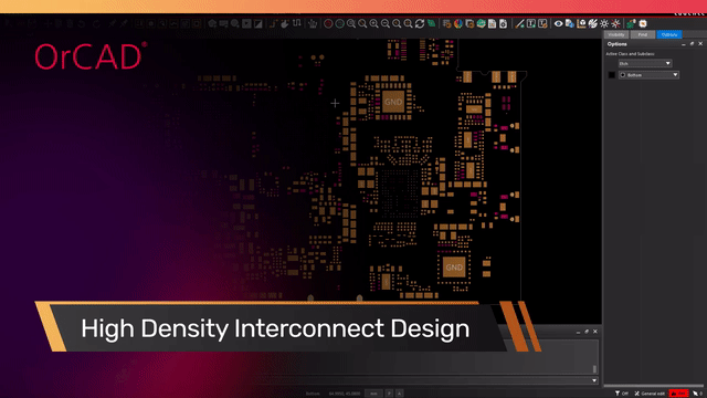
Electronic Interconnects: Maintain Connectivity in a Multi-Board PCB System
Key Takeaways:
-
Challenges with high density PCB interconnects.
-
Types of high density PCB interconnects.
-
Design considerations.
As electronics undergo miniaturization, PCB designers find themselves in need of a new skill: high density interconnect PCB design. High density interconnect PCBs, or HDI PCBs, are characterized by smaller routing spaces, a larger number of thinner traces per unit area, and closely populated components. HDI design also involves micro, staggered, blind, and buried vias on a multi-layer PCB.
Despite featuring a more compact design, HDI PCBs might need to interface with external modules. That is where high density PCB interconnects come in. HDI PCB interconnects allow a PCB to be connected to another PCB directly or via cables. In this article, we will be looking at the challenges of high density PCB interconnects, the types of interconnects, and some design considerations to keep in mind.
Challenges With High Density PCB Interconnects
In HDI design, you’ll find yourself working through two or three main difficulties faced with electronic interconnects. These factors tend to be in frequency and switching speed limitations, current capacity, and operating temperature. Also, the board area is often a luxury in HDI design, which means that interconnects are likely to be surface mounted rather than through holes.
Signal integrity and thermal conductivity considerations are both paramount for any PCB system design, and working through the potential resilience of a chosen connector will involve smart planning and clear documentation.
Let’s take a look at the types of high density PCB interconnects available.
Types of High Density PCB Interconnects
Whether you plan to create vertical towers of PCBs stacked on top of each other or need to load multiple boards into racks to fit into a server, designers have many options when it comes to the types of connectors available.
Standard Board Interconnects: Male/female, pin/socket headers are the most common type of board-to-board connector out there. These interconnects are available in finer pitches to fit HDI PCBs.
Backplane Connectors: A typical backplane is a PCB with no active components. Its primary purpose is twofold: provide structural integrity to the multi-board system and serve as a surface for multiple daughter boards to connect to. Backplane connectors for high density interconnect designs feature denser multi rows of pins and sockets.
Card Edge Connectors: Often used as expansion slots on motherboards, backplanes, or riser cards, edge connectors are designed to mate with the conductive traces lining the edge of another board (e.g., PCI-e slots).
Wire-to-Board: Need to connect cables or wires to a board? FFCs (flexible film cables), FPCs (flexible printed cables), high-speed internal cabled interconnects, and ribbon connectors are just a handful of the options available.
Design Considerations for High Density PCB Interconnects
Now that we’ve covered the different types of PCB interconnects available, let’s take a look at some general design tips to consider when implementing your HDI PCB design.
EMC/EMI
- When stacking two or more HDI PCBs, you’ll want to consider the effects of crosstalk, impedance, and other EMI (electromagnetic interference).
- Beware of common-mode EMI as well—when two legs of a differential pair are different lengths, the difference can create a longitudinal signal in the common-mode, turning the system into an efficient antenna.
- Avoid accidental antennas. When antennas are unavoidable, keep your signal and return currents closely coupled to reduce emissions. In fact, keep all signal layers across the stack closely coupled to an uninterrupted reference plane.
- Keep your signals separate. Analog (DC) and digital (AC), high speed, and low speed circuits should always be kept separate. The same is true across the HDI PCB stack. Be aware of which traces are routed through your boards.
- Remember that the interconnects and vias connecting your boards together change the overall signal of your system. You can read more tips for reducing EMI in your PCB designs here.
Corrosion
Corrosion poses a direct risk to connectivity. Copper, lead, and plated tin are highly susceptible to corrosion. On the other hand, gold, silver, graphite, and copper-nickel alloys are highly resistant to corrosion. Understanding the conditions that lead to corrosion can help you make informed decisions on the types of materials you should use for your connections and components.
- Atmospheric: When metals are exposed to oxygen and water, oxidation can occur. Moisture in the air is all that is needed to corrode copper contacts, reducing conductivity.
- Fretting: Frequent wear and tear in moving parts, such as the wiping action in solder-plated switches, is known to cause corrosion by removing the surface oxide layer and exposing the underlying material to oxidation.
- Galvanic: There is a reason there is a standard for dissimilar metals (MIL-STD-889). When two different metals are in the presence of an electrolyte (such as from a battery), the more resistant metal corrodes faster than the weaker metal (e.g., gold will corrode faster when in contact with tin).
- Electrolytic: It is possible for dendritic growth to occur between adjacent traces in the presence of an ionic fluid. The potential difference between the two traces pulls metal slivers away from each trace, forming a bridge and leading to a short circuit.
Most PCB designs are mainly concerned with atmospheric corrosion and fretting between mating connectors. By understanding the conditions your product may encounter, it’s easier to select materials accordingly.
Mitigating Risks Associated With HDI PCB Interconnects
Connectivity is important, but it is only one piece of the larger puzzle of HDI PCB design. It takes a holistic design approach to ensure that each board and component fits together in a 3D enclosure while avoiding the adverse side effects of EMI, thermal constraints, and corrosion.
That is where Cadence’s suite of design and analysis tools comes in, with powerful simulation and analytical tools to verify your design at any stage. If you’re looking to learn more about how Cadence has the solution for you, talk to us and our team of experts.