Design Rule Check: HDI - Feature Video
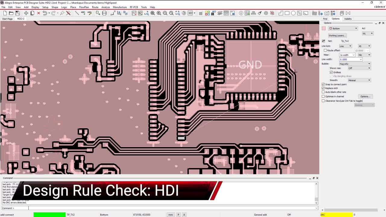
By setting up your HDI rules, you can easily fit more parts per board area and pack more power into smaller form factors.
By setting up your HDI rules, you can easily fit more parts per board area and pack more power into smaller form factors.