Geometric Dimensioning and Tolerancing for the PCB Designer
As we continue to shrink the electronics in our lives, the need for concise documentation grows more important at each node. The dimensions we provide are the determinants of success. If the tolerances are too tight, the cost is going to be higher. Conversely, overly loose tolerances lead to misfit parts that have to be reworked or even scrapped. Geometric dimensioning and tolerancing is a tool we can use to improve the balance between low cost and acceptable yields.
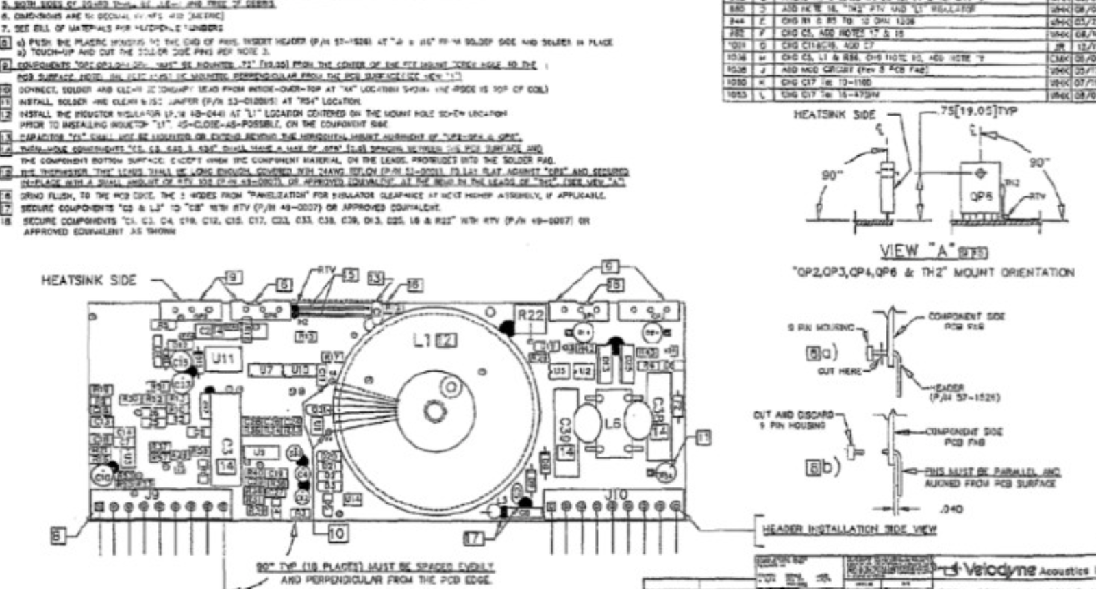
Image credit: Velodyne
The source of the tolerance is often a function of the component selection. Edge connectors, in particular, are notorious for having a data sheet with extreme tolerances that nobody can build. One of my favorite interview questions is about what to do in those cases. Getting to a compromise with the fabricator, the assembly team and the part vendor isn’t always easy but that is the answer I want to hear.
Then, there are vague dimension data points such as a minimum slot width with no maximum value. These unilateral tolerances leave us guessing as to the best nominal size. Making sure that type of information is captured at the board level drawing takes a methodical approach. Setting aside a layer for special instructions has worked for me. In larger organizations, this has to be documented. Even a one-person operation should have some notes on how to handle exceptions.
Reference Dimensions
All dimensions have a tolerance except those noted as reference dimensions. The reason a dimension would be classified as a reference dimension is that it is already described in another location or is based on the total of smaller dimensions. A hard fast rule is that we don’t want to dimension any feature more than once. A reference dimension is noted by a rectangle around the dimension value and would not be measured during a first article inspection.
Tolerance Zones
Traditional dimensions describe the horizontal and vertical numeric values starting at a point of origin. The best point of origin or datum is typically a non-plated tooling hole. Board edges are not so good since the circuit pattern is registered on the hole pattern rather than the board outline. There will be dimensions from the tooling hole to the edges and also from tooling hole to tooling hole. The usual X and Y dimension tolerances establish a square zone of acceptable process variation. If the tolerance is plus/minus five mils then the square of acceptable locations will be ten mils by ten mils centered around the nominal location. Since this literally leads to corner cases, the tolerance would have to be tighter in order to maintain an acceptable fit.
Meanwhile, a “true position” tolerance of the same five mils creates a circle of acceptable hole locations that fit inside the square. This eliminates the corner cases that make the mounting hole pattern prone to misalignment. Further, the positional tolerance can call out more than one datum feature for more meaningful control of the design.
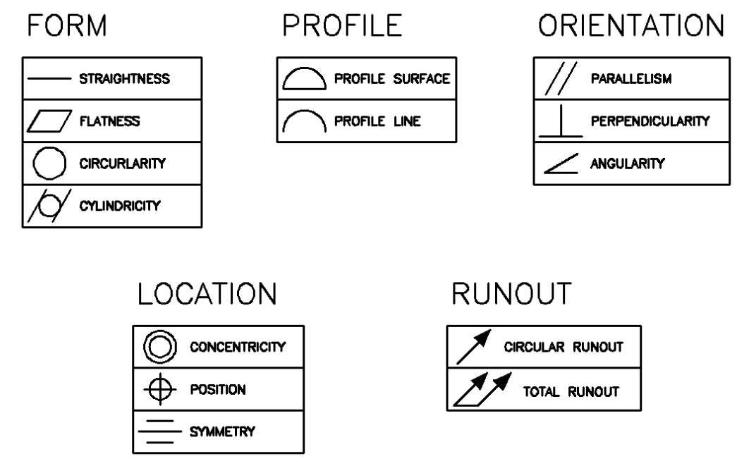
Image credit: ManufacturingET.org
As you can see, there are a number of ways to constrain the geometry. The cross-hair positional target is the most widely used in PCB layout documentation; generally for hole locations. Flatness, Parallelism and Runout are a few other common geometric tolerances applies to PCBs. There are reasons for any of them to show up on a drawing. It all depends on the physical restrictions required for a particular board.
Typically, the folks in charge of the mechanical attributes of the entire product have some misconceptions of what we can do as PCB Designers. We accept that the fab shop can only promise +/- 10% on the nominal board thickness. That is a 12 mil range on an .062” board. Mechanical Engineers would often like less than that.
Putting the restrictive tolerance on the documentation is one thing. Getting delivery on that specification is another. It is up to us to guide the team with respect to what can be reasonably done. From that point onward, we need to provide the vendor with the most concise set of data we can with respect to their strengths and limitations. Geometric Dimensioning and Tolerancing is one of our best tools for that cause.
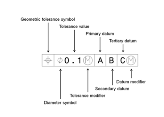
Image credit: Technia
This is a typical geometric tolerance block. It starts on the left with the type of tolerance. Next is the diameter of the circular tolerance zone followed by a modifier that will be one of three conditions; maximum, minimum and nominal size. The A, B, and C are listed to show the anchor points of the dimensions. This tells the inspector what to measure and where to put the measuring tool for the X, Y and Z planes. The tolerance frame is placed in the vicinity of the dimension values.
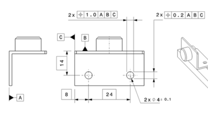
Image credit: Technia
This little bracket illustrates the concepts that were covered above concerning reference dimensions, positional tolerances and datum assignments. The tolerance is different in the X and Y directions. The result is an oblong tolerance zone. Datum -A- (all of them, actually) is an edge and that’s not really an issue on a mechanical part. Positional tolerance can also be called out as a note on the fabrication drawing which is common.
The goal is to sufficiently describe the design such that everything fits together without going to excessively tight tolerance values.