Voltage Regulator Simulation with PSpice in OrCAD X
Key Takeaways
-
Choosing the right regulator type and topology is crucial to meeting efficiency and stability needs in your power design.
-
PSpice simulation in OrCAD X lets you test line/load regulation, dropout behavior, and component limits before building hardware.
-
Simulating feedback and input ripple ensures your regulator circuit will handle real-world fluctuations reliably.
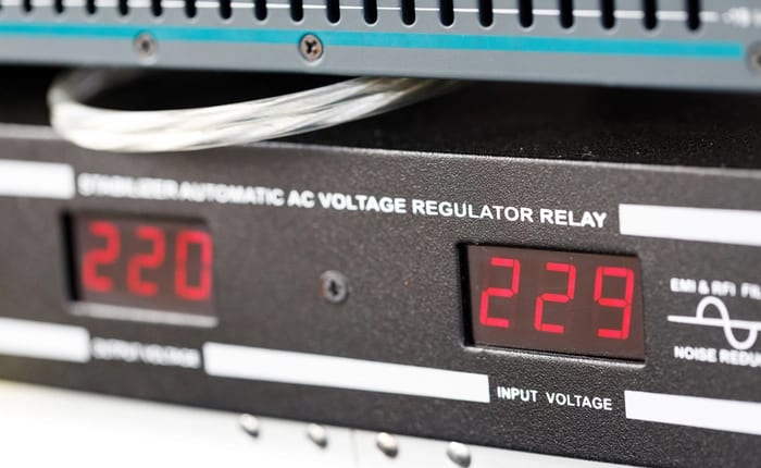
This power supply module contains multiple voltage regulator circuits.
Every new electronic device needs some level of power regulation. Whether a product runs on batteries, an external power supply, or AC mains, you must devise a regulation strategy for your new system. This approach can involve multiple power regulation circuits, often with feedback to provide high-efficiency power conversion. You may need various supporting components and features that help you regulate your power output, especially when the system runs at high power.
Everything from VRMs for CPUs and GPUs to simple linear DC regulators needs some evaluation before layout, and OrCAD X PSpice simulation capabilities can help you spot design problems. Here’s what to watch for in your voltage regulator simulation steps and how you can spot circuit design problems.
Voltage Regulator Circuit Types and Topologies
A voltage regulator circuit topology will determine how the device functions and defines component placement. Each type of voltage regulator circuit and topology provides different advantages and disadvantages. Before you begin simulating your voltage regulator circuits, you must decide which type of regulator you need, the topology, and any other features required to maintain stable power with high conversion efficiency.
Types of Voltage Regulators
There are two fundamental types of voltage regulators you’ll find in electronic systems:
-
Linear regulator: These regulators use a linear resistive element (e.g., a potentiometer) or a nonlinear element operating in the linear regime (e.g., a MOSFET) to provide a stable voltage output. The common types of linear regulators are series, shunt, and low-dropout (LDO). The efficiency of these regulators may range anywhere from 60% to 80%.
-
Switching regulator: These regulators use a switching FET with discharging reactive elements to step up (boost converter) or step down (buck converter) the output voltage as needed for a specific application. They provide high-efficiency DC-DC power conversion, with efficiency easily exceeding 90%. A VRM for a GPU or CPU is a common type of switching regulator.
While each voltage regulator circuit design varies in efficiency and component requirements, combining them in a multi-stage regulator strategy can be highly effective. This type of arrangement can provide higher efficiency power conversion than when a linear voltage regulator circuit is used alone, and it allows the designer to provide power to multiple circuit blocks running at different voltages.
Linear Regulators vs. Switching Regulators
The simplest type of linear regulator is a shunt regulator. This voltage regulator circuit uses a Zener diode to provide feedback between the low end of the load and the high end of the output, thereby providing a stable power output. A series regulator is a variation on this, although a bipolar transistor or MOSFET is used on the high side of the regulator to provide a stable output. The base/gate of the transistor connects to the Zener diode in the feedback loop, which then modulates the base/gate current to a stable value.
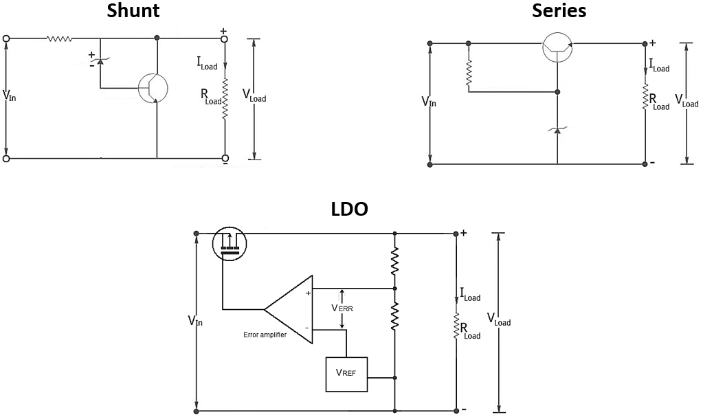
Three common linear voltage regulator circuit diagrams: (Left) shunt, (Center) series, and (Right) LDO.
Switching regulator designs have buck, boost, or buck-boost topologies. The common theme among these circuits is their use of switching transistors to regulate the output voltage and current to specific levels. This action requires sourcing the transistors with a PWM signal to modulate the output current.
Switching regulators and complex linear regulators often include a feedback loop as part of the regulation strategy. For an LDO, the feedback loop consists of a silicon bandgap reference and an op-amp (called an error amplifier in LDO circuit diagrams). For a switching regulator, the feedback loop and control strategy can be as simple as an ADC and MCU to control a PWM signal, or a programmable sensing amplifier for higher power applications.
Feedback and Safety Ratings in Voltage Regulators
In a voltage regulator circuit, feedback is more than providing gain to reach the desired output power. It is also about controlling the regulator if the output voltage and current deviate from the desired value.
Controlling Feedback
-
Switching Regulators: A common strategy in high-power switching regulators is to use a sensing amplifier and an ADC to quantify the output voltage. This method can interface with a programmed MCU to adjust the PWM signal’s duty cycle, modulating the switching FET.
-
Linear Regulators (LDOs): Typically use an error amplifier and a voltage reference (like a silicon bandgap reference) in their feedback loop to maintain output stability.
Simulation for Component Safety
In a simulation, you typically do not need to examine what happens in the feedback loop directly unless you’re using active components. The key is to check that the voltage/current through the feedback loop does not exceed component specifications. Components like current sense amplifiers (in switching regulators) or error amplifiers (in an LDO) will have absolute maximum ratings. You should compare these ratings against the simulated voltage/current in the feedback loop and apply the appropriate safety margin in your design.
Making these comparisons is as simple as using DC sweeps and checking when the input voltage places unacceptable loading on your voltage regulator circuit's components. If your absolute maximum is not up to the maximum DC voltage you intend to use, the components you chose will likely be safe during operation.
For more complex power delivery and regulation systems that will run on AC power, a power factor correction (PFC) circuit may be necessary, particularly when a switching regulator is part of the power circuitry. This additional circuit is placed after the rectifier and smooths out the stepped-up AC current from the input. Suppose the current drawn into the switching regulator stage has unacceptably high total harmonic distortion (THD). You need a PFC circuit on the input according to the European IEC 61000-3 standard.
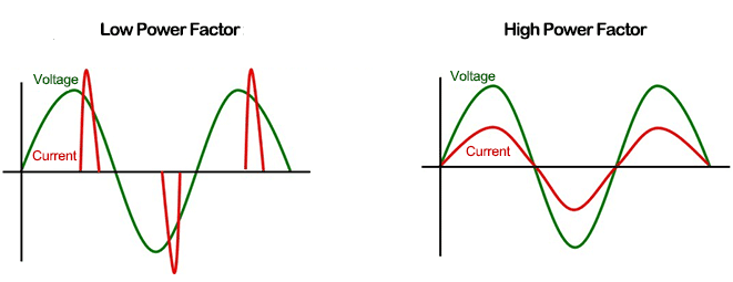
Waveforms you can expect with low and high power factor. A PFC circuit takes the waveform on the left and smoothes out the current drawn by the switching regulator. This action produces the graph on the right, although the current has some superimposed ripple.
Voltage Regulator Simulation with PSpice
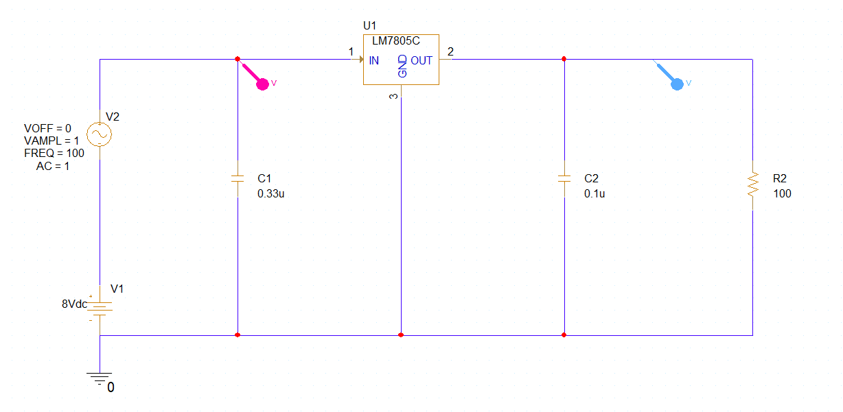
In the example below, we will show how to simulate the performance of the 7855 voltage regulator using PSpice within OrCAD X. The 78XX are a family of self-contained, fixed linear voltage regulators. The last two digits indicate the output voltage, which is 5 volts for the 7855.
Step 1: Project Setup and Select Voltage Regulator Circuit Component
In an OrCAD X Schematic, first, create a new project via File > New > Project, name it appropriately, and critically, check the "Enable PSpice Simulation" box. This selection activates the PSpice menus and toolbar.
Next, build your circuit using PSpice-compatible parts under the Place > PSpice Component menu. You can also search for your part with the Search function. Place PSpice capacitors for C1 and C2, resistor R1, ground, and input sources. We can simulate a DC input with a superimposed AC ripple to test line regulation and ripple rejection. Place a PSpice VDC source and set its value (DC = 8V). Place a PSpice VAC source in series with the VDC source (ensure its DC offset is 0V) and set its amplitude (AC = 1V, AMPL = 1V) and frequency (e.g., 100Hz).
Step 2: Wire the Circuit
Use the 'Wire' tool (Place > Wire) to connect the components according to your design. Ensure all nodes are correctly connected and save the schematic.
Step 3: Configure the Simulation Profile and Place Probes
-
Profile: Create a New Simulation Profile, select Time Domain (Transient), and set Run to time (e.g., 100ms).
-
Probes: Place voltage markers on the input node (after sources) and the output node, like in the image.
-
Run: Execute the simulation (PSpice > Run).
Step 4: Interpreting Simulation Results
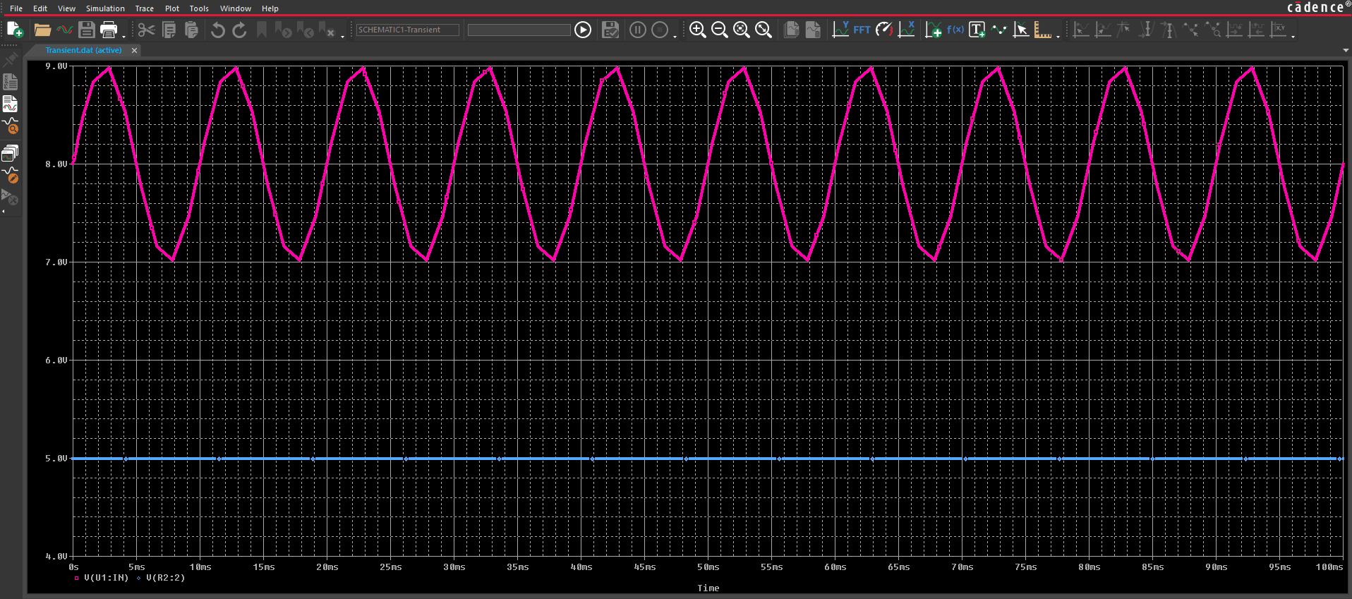
Scenario 1: Sufficient Input Voltage (Vin = 8V DC ± 1V AC):
The waveform viewer shows the input voltage fluctuating (e.g., pink trace) between 7V and 9V. The output voltage (e.g., blue trace) should remain stable at 5V, demonstrating good line regulation and ripple rejection (PSRR). The regulator successfully handles the input variation.
Scenario 2: Input Voltage Insufficient (Dropout Test):
Go back to the schematic and change the VDC source value to 7V. The input now swings between 6V and 8V. Re-run the simulation.
As the input dips below approximately 7V (Vout + Dropout Voltage, roughly 2V for the 7805), the output voltage will fail to maintain 5V and will start to follow the input ripple during the troughs. This response simulates the regulator entering dropout. Linear regulators require this minimum voltage headroom (Vin > Vout + Vdropout) to function correctly.
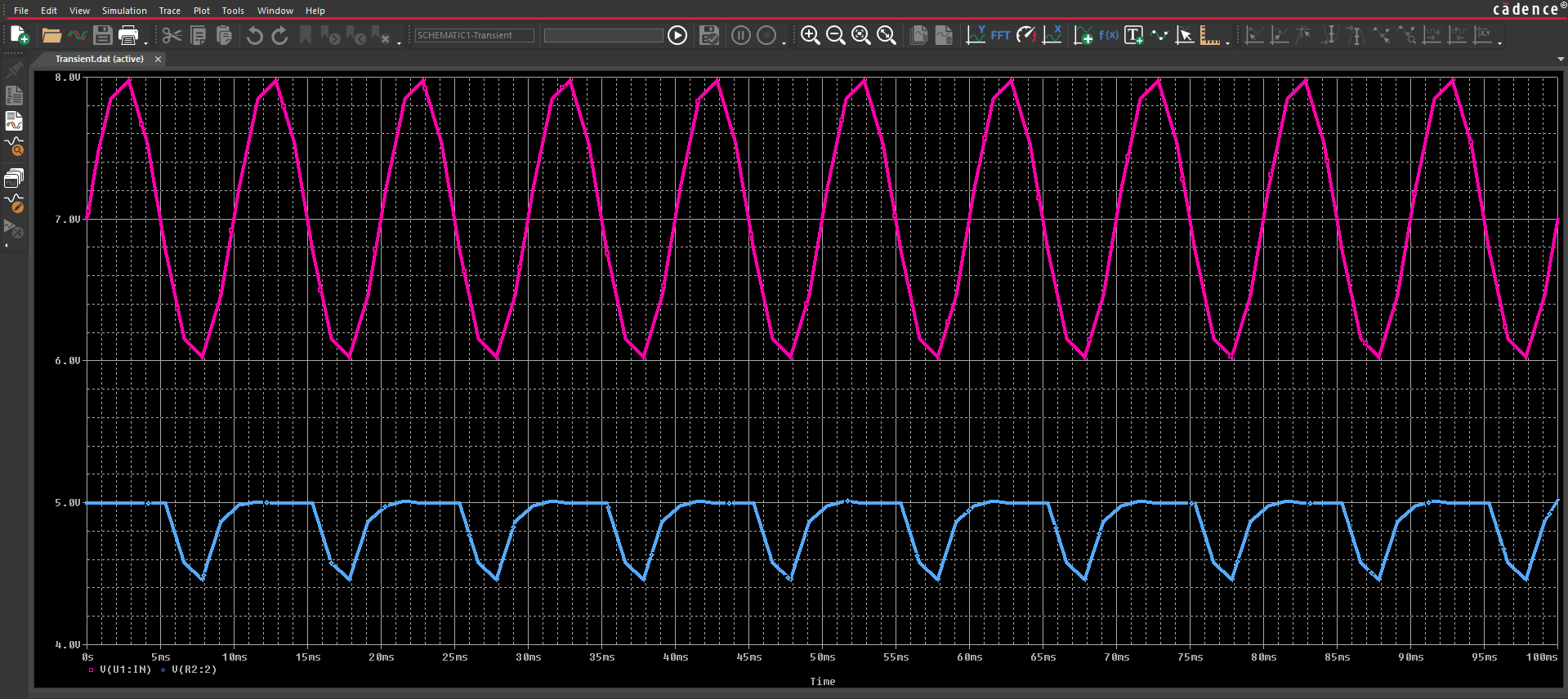
Input and Output Voltage Simulation Results for Scenario 2
This simulation visualizes the regulator's operational limit and confirms the necessity of maintaining adequate input voltage for stable output.
Designing reliable power delivery systems requires careful verification. Voltage regulator simulation using PSpice within the OrCAD X environment is critical in this process. It allows engineers to analyze line/load regulation, ripple rejection, dropout voltage, transient response, and component stress under various conditions before committing to hardware. Ready to validate your power designs? Try OrCAD X for free, including PSpice simulation capabilities, or explore the complete OrCAD X platform to leverage comprehensive simulation tools for your voltage regulator circuits.
Leading electronics providers rely on Cadence products to optimize power, space, and energy needs for a wide variety of market applications. To learn more about our innovative solutions, subscribe to our newsletter or our YouTube channel.