PCB 101: What are Blind and Buried Vias
Sometimes, you can’t fit all your connections on one layer. This is where vias come to your rescue!
Vias are barrel shaped vertical conductive holes that make connections between multiple layers of a PCB. The IPC defines eight different types of vias, but we’re going to talk about blind and buried vias; the two you’re most likely to work with.
A blind via connects an outer layer of the board to inner layers and doesn’t go through the entire board. A buried via connects inner layers without reaching the outer layers. And a through hole via goes all the way through, from top to bottom, connecting all layers.

Source: EEVblog
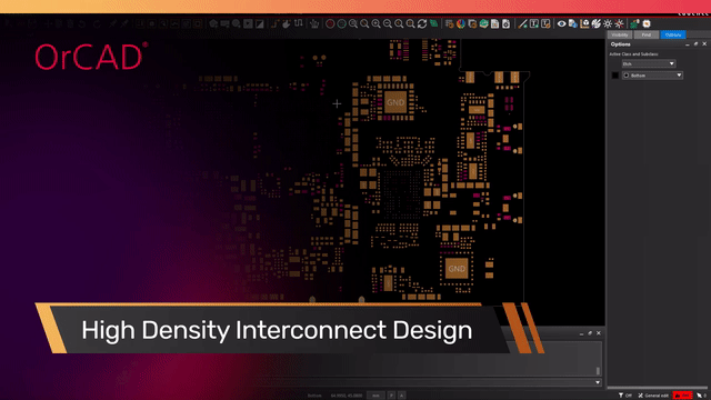
Fitting More on Smaller Boards
Blind and buried vias provide electrical connections from the outer layers to the inner layers as well as in between the inner layers, and are used when you have limited space on your PCB. Buried vias are hidden beneath the layers and free up surface space without impacting the traces or surface components on the top or bottom layers. Blind vias also free up space, can be essential for fine pitch BGA components and have the added benefit of helping reduce signal stubs through the drilling process as the via terminates at the last connected layer.
You mostly see blind and buried vias in High density interconnect (HDI) PCBs. HDIs provide benefits such as increased layer density, improved power delivery and use of much smaller pitch devices. The hidden vias help keep the board light and compact. It is common to see blind and buried vias in electronic products like, cell phones, laptops, and medical devices to name a few.
Incorporating blind and buried vias make more connections and higher board density possible. But not without drawback. Vias add extra steps to manufacturing and testing, which come with added costs.
How Do They Make These Things?
Vias are manufactured in two ways: either after or before multilayer lamination. When blind and buried vias are created, one or more of the cores are drilled and the through holes are plated. Then the stack is built and pressed. You can read more about the manufacturing process in the IPC-2221B manual.
When creating blind vias, it is important to be aware of the drill depth. Depending on how shallow or deep the hole is, it could have a negative impact on the board. If the hole is too deep then it may cause signal distortion or degradation, and if it’s too shallow then it could result in an improper connection.
It’s best to consult with your PCB manufacturer to get advice on the best approach to design your board to avoid a costly manufacture. Make sure to have your manufacturer plug the vias with either metal or thermal/electrical epoxy and plate copper over it; or else internal air bubbles can migrate upwards and lead to voids or pin holes in the solder joint.
Blind and Buried Vias Within Layout
You can easily configure your vias within the constraint manager in the physical workspace. Standard clearance rules apply when placing the vias. It is not recommended to place a via directly between pads of a surface mount component (SMD) as solder flux could potentially get trapped and cause corrosion problems. If solder flux would be under the SMD, inspecting and diagnosing the issue between a pad and via would be difficult once the board is manufactured and assembled.