Plating Considerations For Printed Circuit Board Assembly
In the United States, the pale green skin of the Statue of Liberty is as iconic as the International Orange of the Golden Gate bridge; some of our favorite earth-tones. The thing is that the green is really the result of benign neglect. Strip away the oxidation and Lady Liberty looks like a shiny new penny. I’m having trouble even picturing that.
This is relevant to us as a reminder that exposed copper will corrode very quickly in the atmosphere we all need to survive. The construction of a PCB is going to include outer layers of copper for component attachment and fan-out as a minimum. One of the first things that happens is a plate-up of those layers with more copper that also plates the through-holes (vias) for that board.
Copper Plus Copper - A Fabrication Process Norm
Rigid PCB stack-ups usually do not account for this plating step. The designer is counted on to envision the construction sequence as they allocate copper to various layers. Layers where core-vias start and end will face the same process as the outer layers in this regard.

Figure 1. Image Credit: Cosmos - a rendering of an early stage of copper oxidation.
When it comes to the stack-ups for flexible printed circuits, the additional plating is normally documented in the stack-up diagram. The added copper stiffens a flex and that may be undesirable. That being the case, we would look into button plating which is more selective than panel plating. As a rule, all plating, masking, covering, marking and stiffening on an FPC is going to be a material designed for that purpose.
For an FPC, the copper itself is annealed, that is to say softened by passing the sheet through two big rollers that squeeze it down again and again. This creates a granular alignment that provides a smooth outer surface for the traces that actually improves signal integrity. It is specified as “rolled annealed copper” or just RA cu. for shorthand.
More copper is thus the first plating operation. Whether it shows up as a separate item or not, it has to be a factor, particularly as we lean into high density interconnect and controlled impedance situations. Whether it is rigid, flexible, or a combination of the two, the weight of the copper is one of the main considerations for the performance of the circuit board.
Notes on Usage: Most of these finishes will be measured in micro-inches or microns but copper has its own unit of measure based on the weight of one square foot of the copper. Flattening one ounce of copper to fill a square foot of space will end up with a sheet that is 0.0014 inches thick. Two-ounce copper will be twice as thick. You’ll find base materials from a quarter-ounce on up to multiple ounces though the thinner copper is more common.
The entire printed circuit board is a balancing act between signals and power distribution. It’s common for different weights to be used as long as they use a bookmatched sequence that looks the same whether it is read from top to bottom or bottom to top. The thicker outer layers of copper will want to be covered with something as soon as possible so it doesn’t turn green.
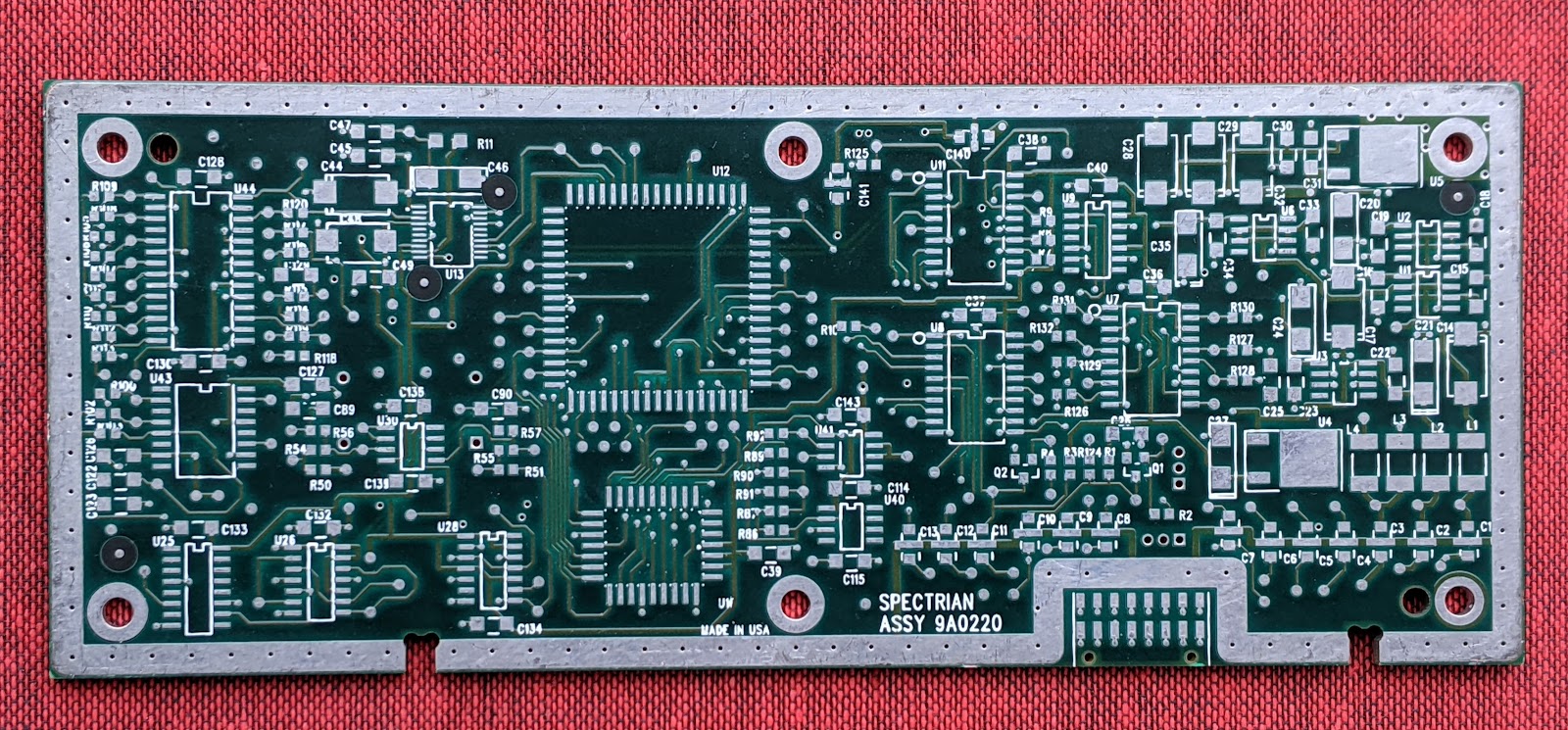
Figure 2. Image Credit: Author - Hot Air Solder Level (HASL) finish on a DSP board, bottom side, circa 1996.
The highest reliability solution is still the old solution of using Sn63 tin/lead for hot-air-solder-leveling or HASL for short. This stuff has been banned for a long time and an exemption is required for its use. Still, there is nothing proven to be better for orbiting satellites or other scenarios where long-term operation is required. The list of exemptions remains stubbornly long. Lead based solder does not meet RoHS environmental requirements so disposal is the main issue here.
Dissimilar Metal Over Metal to Protect Bare Copper
Precious metals are not as easy to obtain or work with but those are the leading partners for plating in today’s consumer market. Gold does not readily bond with copper. Using an intermediate layer of nickel solves this intermetallic issue and is the formula we know best for surface-mount components with via-in-pad technology. Electroless Nickel / Immersion Gold (ENIG) is a very popular finish because it takes to solder really well and does a commendable job of protecting the copper prior to soldering.
“The more the pads look alike, the better in terms of consistent solder joints.”
Another benefit of ENIG plating is that the vendor can achieve a flat pad surface. The effect is increased assembly yields vs. HASL which leaves more surface roughness around the via-in-pad construction. The more the pads look alike, the better in terms of consistent solder joints.
There is a known downside to ENIG finish in the form of an assembly defect known as black pad. It is a breakdown of the nickel barrier leading to open or intermittent circuits. I believe this was mostly solved as the metallurgists fine-tuned the phosphorus content. There were growing pains with the process back then but this defect isn’t common.
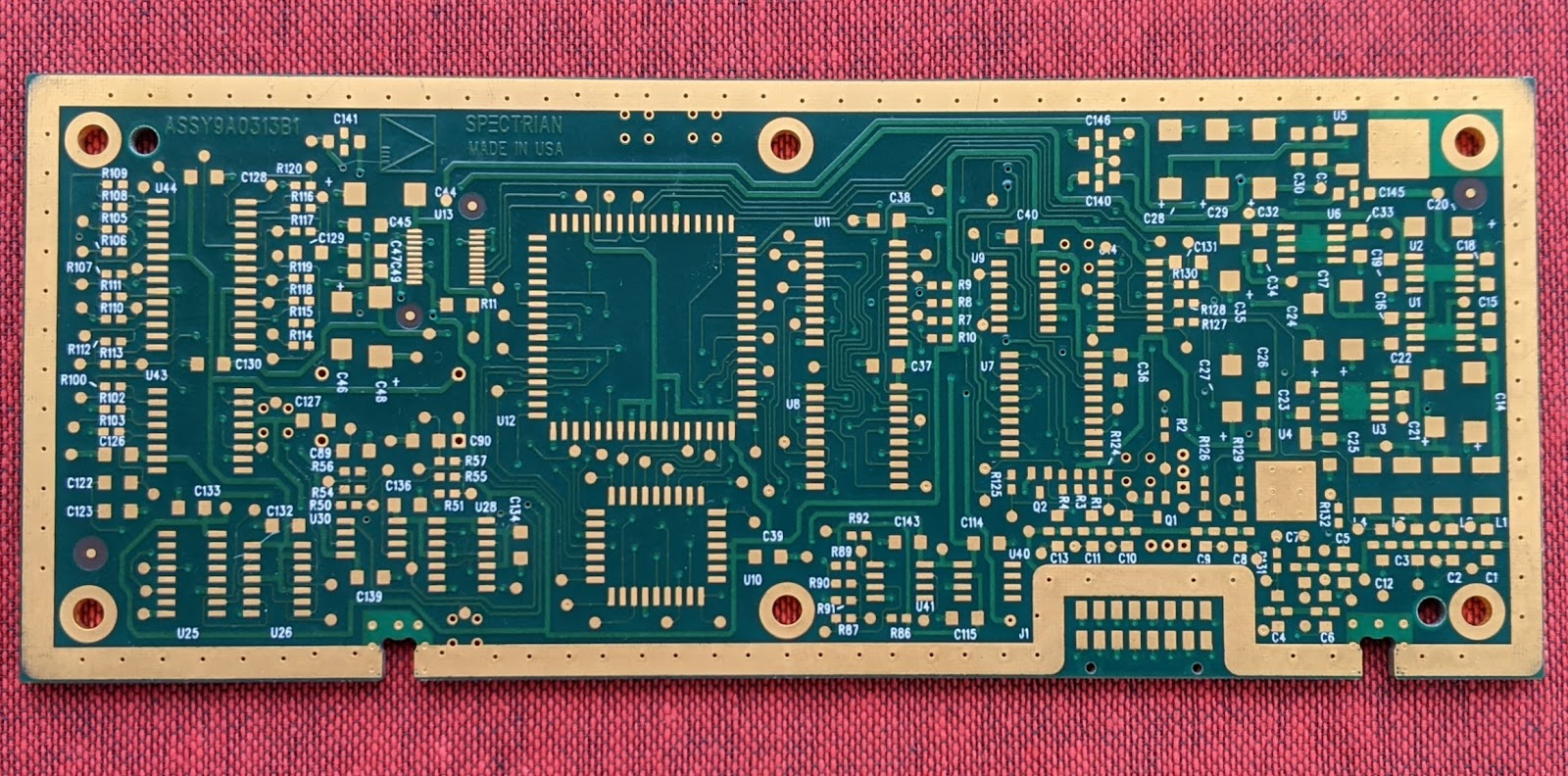
Figure 3. Image Credit: Author - The 1997 DSP iteration when we learned to spend a little more on the bare board and save money overall with improved assembly yields.
Hardness matters on these gold finishes. ENIG produces a medium hardness that is fine for general purposes. A more durable hard gold is recommended for gold-finger edge-connectors or push-buttons. On the other hand, attaching wirebonds for chip-on-board applications takes a softer gold. Both of these may require more expensive selective finishes. Perhaps not; read on.
Palladium as an Additional Barrier Metal Layer
One way to implement wirebonds on a circuit board is to use ENIPIG which is similar to ENIG but adds a layer of palladium between the nickel and the gold. The palladium isn’t cheap but it reduces the amount of gold which is even more costly so, on balance, it’s a win. It’s very solderable, has tremendous shelf-life and meets the pull-test requirements for reliable wirebonds. ENIPIG is a versatile protector of copper.
As an environmental coating, tin is still in the game but with a new partner. While traditional solder is 63% tin, the newer formulations are closer to 97% tin with the main “impurity” being silver. Other trace metals can also be added to suit different processes including keeping tin whiskers in check which is common with pure tin.
The primary difference with tin alloys minus the lead is the higher melting point. The components and the boards themselves have to withstand much greater reflow temperatures with these ‘green’ materials. The industry as a whole moved from tin/lead to gold/nickel for lead free compliance and then to tin/silver coatings to comply with Reduction of Hazardous Substances mandates.
Organic Surface Protectant - A Low-Cost Solution
A low-cost alternative to plating additional metals to the bare copper is to apply an organic surface protectant (OSP) over the exposed copper. An OSP is a super-thin coating that protects the otherwise bare copper until the solder takes over. As a replacement for various plating processes, OSP is meant to vaporize during reflow without any residue.
Notes on usage: Until they are soldered, bare boards should be vacuum sealed and kept in humidity-controlled storage. A piece of release paper should be packed between each board to reduce the chances of scratching the surface protectant. Sunlight also breaks down this type of protection so proper storage should be indoors. You don’t want to wait too long to process OSP coated boards in any case. As far as I can tell, there is no ratified IPC spec regarding OSP though there are multiple committees working on preliminary specifications.
One other thing to note is that there may be exposed copper pads on a board that do not get soldered. Test points and other exposed metal will benefit from a solder paste opening in the stencil. That way, the test point gets a nice coating of solder over the copper after the OSP is gone. That would not be required with plating solutions but a little extra material where the test probe hits isn’t going to hurt things.
There are all of these plating options and details that splinter the choices even further. Generally speaking, use gold for high density and high speed applications and go with tin based coatings for more traditional boards including surface mount without via-in-pad technology. Lastly, possibly skip the added plating steps altogether by using OSP coatings for mass production.