Optimizing PCB Design and Prototyping With OrCAD X
Key Takeaways
-
From research and component selection to schematic capture and SPICE simulation, each step in PCB design and prototyping is crucial for ensuring the final board meets design specifications.
-
Various prototypes like visual models, proof-of-concept, working, and functional prototypes cater to different testing and validation needs.
-
OrCAD X enhances PCB prototyping with tools for backdrilling, real-time design checks, and interactive routing, streamlining the design process.
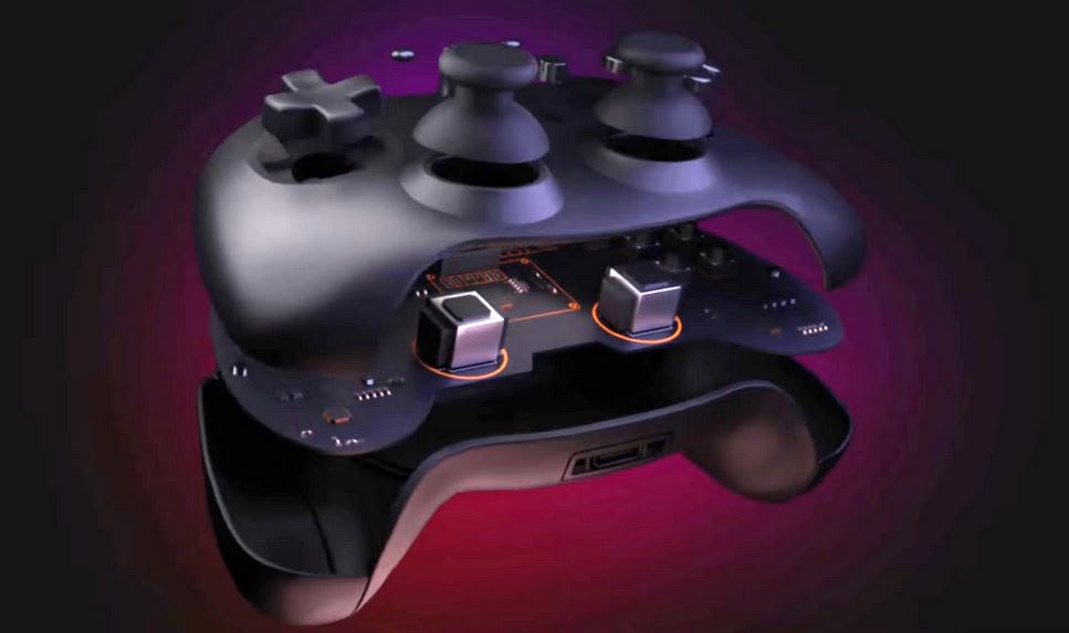
Prototype controller designed in OrCAD X
PCB design and prototyping are two major stages in device production. Prototyping typically marks the end of a design phase, which is crucial for the testing stage, where hardware is tested to ensure it meets the design specifications. Once the design is confirmed as effective, it progresses to the next phases of product development.
When ordering a prototype PCB, manufacturers typically limit the batch to between 1 and 100 units, allowing for effective testing without unnecessary costs. The production of PCB prototypes is quick because only a few units are needed. Typically, all required prototypes are manufactured within a few business days, accelerating design evaluation and adjustment.
PCB Design and Prototyping Steps
Prototypes are particularly useful for testing design concepts or conducting quality assessments of the board. The prototyping phase can be divided into the following key steps:
PCB Design Flow Steps
|
Step |
Details |
|
Researching Parts |
Engineers research parts using various methods to ensure they meet circuit requirements before designing begins. |
|
Component Selection |
Engineers select components based on the required specifications of the circuit. |
|
Schematic Capture |
Engineers place symbolic representations of components and connect them in a visual diagram to conceptualize the circuit's functionality. |
|
SPICE Simulation |
This industry-standard simulation evaluates the behavior of components within a virtual environment, allowing for advanced analysis and visualization of the circuit's performance early in the design process, thereby reducing errors. Cadence PSpice discussed later in the article, enhances this process with its comprehensive simulation and verification capabilities. |
|
Board Layout |
After completing the schematic, it's translated into a board layout where each symbol is linked to a footprint showing the component's physical dimensions. The board is designed to its final prototype form with part placements and connections. |
|
Fabrication Export |
The board layout is exported for fabrication, marking the transition from design to physical creation. |
|
Prototype Validation |
Once fabricated, the prototype undergoes testing to validate its performance. This involves ensuring that the actual performance aligns with both the simulated outcomes and the design specifications. If the prototype doesn’t meet the design specifications, designers return to the earliest step required to solve shortcomings. |
|
Handoff to Product Development |
After successful validation, the prototype is advanced to product development for final adjustments and preparations for mass production. |
When to Create a Prototype
Prototyping is crucial when introducing new products or features, as it allows the design team to refine functionalities and resolve potential issues early in development. Prototyping is also useful in testing, including quality assurance and environmental conditions, to ensure reliability before market release.
For complex projects, prototyping helps identify and troubleshoot issues, significantly improving product quality. Additionally, in situations where only a physical representation of the PCB is required for visualization or discussions, creating a basic material prototype offers a cost-effective solution without the need for a fully functional board.
Types of PCB Prototypes
Various PCB prototypes are utilized throughout the design process to assess different elements of the design. A design team might employ several types of PCBs at different project phases, including:
-
Visual models: These models display the physical layout and structural arrangement of components on the PCB. Generally created first, visual models facilitate easy and cost-effective discussions and reviews of the design's physical appearance.
-
Proof-of-concept prototypes: This simpler type of prototype focuses on demonstrating the core functionality of the board, although it does not include all the features of the final product. Its main purpose is to validate the feasibility of the design concept.
-
Working prototypes: These fully functional prototypes incorporate all intended features and functions of the final product. They are primarily used for detecting design flaws or weaknesses, although their appearance may not closely resemble the final product.
-
Functional prototypes: Designed to closely mirror the final product, functional prototypes offer a realistic preview of the design's appearance and operation, albeit made with cheaper materials to reduce prototyping costs.
How OrCAD X Assists in PCB Design
|
Feature of OrCAD X |
How It Aids PCB Design and Prototyping |
|
Backdrilling Rules and Real-Time Checks |
Automates and checks for clearances, ensuring compatibility with high-speed designs and reducing the need for manual re-checking. |
|
Constraint Manager |
Offers real-time validation of design rules, ensuring compliance with physical and electrical constraints, which is crucial for first-time success and reducing rework. |
|
Rigid-Flex Design Support |
Provides specific tools and design rules checks (DRCs) for emerging rigid-flex substrates, crucial for modern electronics like wearables and IoT devices. |
|
High Speed Awareness With Dynamic Differential Pair Phase Control |
Facilitates advanced handling of high-speed circuits, helping to manage complex differential pairs and signal integrity early in the design. |
|
Real-Time Dynamic Copper Shape Technology |
Offers real-time copper pour plowing and healing, eliminating manual voiding and rework and significantly speeding up the prototype development process. |
|
High-Speed Constraints-Driven Autorouting |
Automatically adheres to strict high-speed constraints, optimizing the routing process for complex interfaces like DDR and PCIe. |
|
3D Display and Visualization |
Provides a realistic view of the design, helping with mechanical integration and clearance checks before manufacturing. |
|
MCAD-ECAD Collaboration |
Facilitates integration and synchronization between mechanical and electrical design teams, enhancing design efficiency and reducing rework. |
|
PSpice |
Allows for advanced circuit simulation and analysis, verifying the performance and functionality of the design before prototyping. Combines industry-leading native analog, mixed-signal, and analysis engines to deliver a complete circuit simulation and verification solution, offering more than 35,000 parameterized models for various devices from major manufacturers |
These features collectively make OrCAD X a powerful tool for addressing the comprehensive needs of PCB design and prototyping, ensuring efficiency, accuracy, and speed from design conception through to manufacturing readiness.
Start your free trial today and explore advanced PCB design and prototyping tools firsthand. See how OrCAD X can streamline your product development process!
Leading electronics providers rely on Cadence products to optimize power, space, and energy needs for a wide variety of market applications. To learn more about our innovative solutions, talk to our team of experts or subscribe to our YouTube channel.