PCB Stacking Techniques for Board Layers in Layout
Key Takeaways
-
Circuit board layer stackup changes will impact manufacturability and the cost of the board.
-
Signal and power integrity details to consider with the configuration of your layer stackup.
-
Different PCB stacking techniques and how your design tools can help get you there.
Spacing circuit board layers apart for clarity is one PCB stacking technique
Most of us don’t know what goes into the different products and devices we use in our daily lives. Your car shifts effortlessly between gears, but do you know how an automatic transmission works? It is not surprising that the majority of electronics users have no idea what it takes to build the complex circuit boards at the core of many of their devices. For those of us designing PCBs, however, understanding how to use and design for different layer configurations is essential.
Circuit boards are much more than a simple platform that supports and connects an array of electronic components. The signal and power integrity of the circuitry in a circuit board can be greatly affected by how the layers of the board are configured. This layer arrangement doesn’t impact just the electrical performance of the board; it will also determine how the board will be manufactured and at what cost. Let’s take a deeper look at this topic to see how different PCB stacking techniques will impact a board and what designers need to know to work with them.
The Three “M’s” - Materials, Manufacturability, & Money
Each layer of a circuit board can only contain a finite amount of routing on it, so it stands to reason that the more nets in your design, the more layers you will need to route them. But, before you start adding layers to your design, it is important to take a step back and look at the bigger picture. The first detail you should consider is the fabrication of the board itself. The layer count of a circuit board is affected by (or will have an effect on) its materials, manufacturability, and the money it will cost to build it.
Materials
A standard digital/analog circuit board fabricated with FR-4 is a known quantity, but if your board is using more exotic, high-speed materials, changing the layer count could create some challenges. Although these materials are better for controlled impedance, signal performance, dimensional stability, thermal management, and much more, they can be difficult to work with and will cost more to build the board. Before you throw in an extra layer pair, make sure you understand all the implications first.
Manufacturability
The higher the layer count in a circuit board, the more complex the fabrication process. Not only will this impact the time and money it will take to build the raw boards, but it could change the yields promised by the fabricator. Before you commit to additional layers, make sure that your manufacturers are on board with your decision as well.
Money
Each layer pair that you add to a circuit board will increase its costs. In general, you can expect to see up to a 40% increase in fabrication fees by going from two layers to four, or from four to six layers. After that, it lowers a little to 35% or 30%, but it will still affect the bottom line of your budget. And, while this may not seem like a big deal when you are in the prototyping stage, don’t forget that this price needs to be extended throughout the production life of the board for each board built.
On the other hand, in some cases, adding layers can save you money. Depending on the complexity of the routing in the design, it may end up saving you money to add extra layers and shave time off your development budget. Extra layers may also allow you to alter the number and sizes of holes, trace widths and spacings, and board size and thickness—all of which could potentially save fabrication time and expense. Using extra layers may also end up being the only way to add more components to the design. The important thing, as we said initially, is to take a step back and look at the bigger picture first. This is even more essential when it comes to how the layer stackup will impact the electrical performance of the PCB.
Components on a circuit board with multiple layers of routing displayed beneath them
PCB Electrical Considerations
A two-layer circuit board is going to have to share surface layers with the components that are placed on it, so, adding layers can give you more room for parts. In addition, there are other areas of the design that will benefit from adding layers to the board.
Signal Routing
For designs with a lot of nets, a multi-layer circuit board is usually the only option to complete the trace routing. In addition, the extra layers will help with the following:
-
Crosstalk: When traces are all jammed together on one layer, the potential exists for those traces to couple with each other and create noise. Adding layers to the board allows those sensitive nets to be spread out as well as to be routed perpendicularly on adjacent layers.
-
EMI: Additional layers allow designers to separate routing layers with ground planes to reduce EMI susceptibility and emissions.
-
High-speed: Transmission line routing can also make use of the extra layers if they are used as reference planes to ensure a clean signal return path.
Power and Ground Planes
Many components on circuit boards require multiple voltage levels for their power requirements. Trying to maintain good power integrity on a two-layer circuit board, where all of this power has to be run with individual traces, can be challenging. Using the extra layers in a board for additional power planes helps resolve this problem. Even with multiple voltage levels on the board, the power planes can be split to manage the different power requirements of the components.
One of the main benefits of additional layers in a circuit board is the ability to configure multiple ground plane layers. In addition to helping improve the power delivery network of the board, the ground planes serve as a reference plane for signal return paths. With two-layer designs, these return paths are often restricted to ground traces and can cause a lot of signal integrity problems in the board. With the dedicated reference planes in multi-layer boards, though, high-speed routing can be on a layer directly adjacent to its reference plane for a clean signal return.
Signal Integrity
High-speed designs usually require microstrip or stripline layer configurations for routing sensitive transmission lines. While microstrip configurations are routed on an external layer, stripline configurations require internal routing layers and ground planes that can only be achieved with multi-layer designs. You can see some examples of these PCB layer configurations in the illustration below.
At one time, increasing the number of layers in a multi-layer circuit board was only to create space for routing additional nets on the board. Now, however, a good multi-layer stackup configuration has to be designed to protect the board from being victimized by external noise sources and prevent the board from propagating them as well. Next, we’ll look at some of the PCB stacking techniques that can be used in multi-layer designs.
Examples of microstrip and stripline routing layer configurations
Different Layer Configurations and PCB Stacking Techniques
Multi-layer circuit boards start at three layers and go up until they are limited by the width of the board and manufacturing technologies available. Typically, designers will choose between four, six, and eight-layer boards. Here are some examples of the layer configurations within those boards.
Four-Layer Boards
There isn’t much variation in a four-layer board. Usually, these boards will have a mixture of solid metal planes and routed power and ground. In some cases, there may be one complete ground plane on an internal layer, or power and ground fills are used on the exterior layers with signal routing internally.
Six-Layer Boards
The traditional six-layer circuit board stackup has been arranged as top, signal, ground plane, power plane, signal, and bottom. This configuration provides very poor signal integrity, as the internal signal layers are not between two planes, and it will create a lot of EMI. A better configuration is as follows:
-
Top signal
-
Ground plane
-
Inner signal
-
Inner signal
-
Power plane
-
Bottom signal
This configuration offers a much cleaner signal integrity solution as long as the sensitive traces are kept on the internal signal layers. This way, transmission lines can use the adjacent power and ground layers as their reference planes, although they still don’t have a symmetric stripline configuration to leverage. One of the best six-layer stackups swaps out an inner signal layer for another ground layer to create the stripline configuration. The problem, of course, is that an entire routing layer is lost, but the board will have better signal integrity protection built into it for high-speed designs.
Eight-Layer Boards
As layer counts increase, the number of possible variations will grow, so we won’t look at different variations. Instead, here is one eight-layer board stackup that will provide good signal integrity protection:
-
Top layer
-
Ground plane
-
Inner signal
-
Power plane
-
Ground plane
-
Inner signal
-
Power plane
-
Bottom layer
The task now is how to set up these board layer stackups, and that is where your PCB design tools can help.
Using Cadence Allegro PCB Editor’s Cross-Section Editor to set up the layer configuration in a PCB design
Leveraging the Power of PCB Design Tools
To create multi-layer configurations for circuit board designs, PCB CAD tools usually have an editing tool or feature that makes the job easier. In the picture above, you can see an example of the Cross-Section Editor that is available within Cadence’s Allegro PCB Editor. With this tool, you can input the values of board layer details such as width, material, and dielectric constant. The editor also shows you a side view of the layer stackup for an easy reference of how the layers are configured and the depth of blind and buried vias. Another useful feature in Allegro is the 3D canvas, which gives designers a much better view of how their design layers interact with each other.
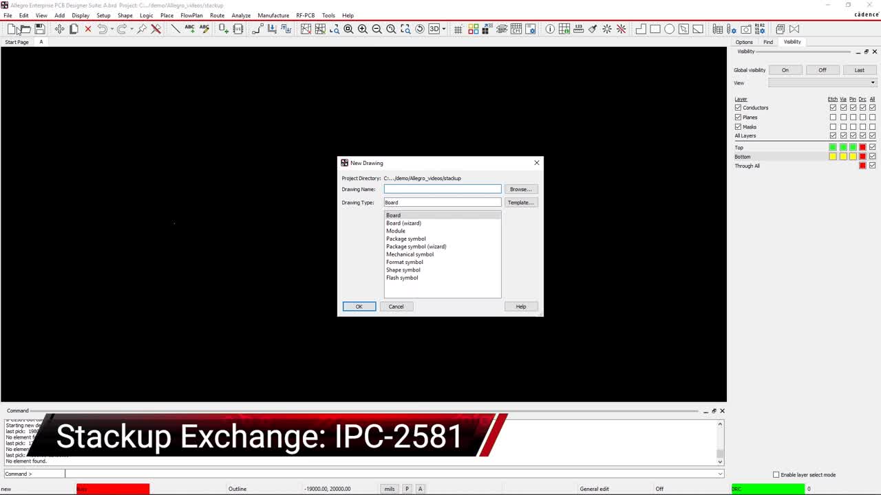
Another very important resource for PCB designers is their circuit board manufacturer. These people have built their business around configuring and building board layer stackups for their customers and they know what they are doing. They will be able to advise you of the best PCB stacking techniques for your design type, desired materials, and cost. In many cases, PCB manufacturers can use your information to formulate the best PCB layer stackup, and then send that data directly back to you for your CAD system. Using the IPC-2581 interface makes communication between design and manufacturing much easier to pull in layer stackup information and send out completed manufacturing files.
For more information on PCB stacking techniques, check out the two-part E-book series on stack-up strategies. Click here for Part 1 and Part 2.
If you’re looking to learn more about how Cadence has the solution for you, talk to us and our team of experts.