PCB Layout Guidelines for Switching Power Supplies
Key Takeaways
-
Potential problems with power supplies in PCB layouts.
-
Setting up PCB parameters for power supply layout.
-
Component placement and routing tips for an optimum layout.
The component layout of a circuit board.
No matter what the function of a circuit board is, it will need power to operate, which is usually generated by an onboard power supply. There are two types of power supplies that are typically designed into a circuit board: linear and switch-mode. With simpler circuitry and lower component costs, linear supplies provide a reliable source of power. The problem is they are also inefficient, which is undesirable in circuit boards that require higher levels of power.
To supply the increased power demands of most circuit boards, a switch-mode power supply (SMPS) will be used instead. There are different types of SMPSs and they can be configured to output different voltages and currents depending on the need of the circuitry. A switch-mode power supply is very efficient in its operation but it also can cause a lot of problems for the circuit board, such as electromagnetic interference (EMI), if it isn’t laid out correctly. To help you avoid these problems, here are some layout guidelines for switching power supplies.
Problems with Incorrectly Laid Out Switching Power Supplies
A switch-mode power supply is often the preferred way to generate power on a printed circuit board. Using a switching regulator to convert the power, an SMPS will generate current more efficiently and with less heat than a linear power supply, which relies on larger heat-producing parts. However, the normal switching operation of the SMPS has the potential to radiate noise, which if not controlled properly, will add to or create the following problems:
-
Electromagnetic interference: The switching of the voltage in an SMPS between the on and off states can create electromagnetic interference. Not only can EMI interfere with other electronics external to the circuit board, it can also disrupt the circuitry on the board. EMI can degrade the signal and power integrity of the circuit board to the point of causing intermittent problems or outright failure.
-
Ground bounce: The rapid switching activity of the SMPS can impact the ground node of a circuit board, bouncing its reference ground level higher than it should be. With this artificially high ground level, other signals may switch incorrectly resulting in false data being transmitted in those circuits.
-
Power ripples: Another problem with the switching of a power supply is that it may form power ripples which could create crosstalk in nearby circuitry. This crosstalk can overpower a weaker signal, which could result in the disruption of that circuit.
As we have seen, these potential noise problems from switching power supplies can cause a lot of power integrity issues for your circuit board. To avoid these problems, it is important to follow good power supply layout guidelines starting with how the board will be configured in the layout tools.
Many parameters can be set up for your layout, including thermal reliefs on power and ground planes.
Circuit Board Layout Parameters for Switching Power Supplies
To ensure good power integrity in your design, a circuit board should be laid out with a clear plan for the power delivery network (PDN). This way, your final design will end up with a PDN that can provide clean and uninterrupted power to all components without creating interference. To do this, the first PCB parameters that must be set up are the board layer configuration and stackup.
It is important to start with a schematic that is far enough along in its development so that all power supplies on the board are identified. From that information, you can begin to configure the layer stackup for the best signal integrity and power integrity of the board.
This will mean positioning power and ground planes for the best signal return paths, controlled impedance routing, and power supply isolation. Often, your circuit board manufacturer can help with these decisions as they routinely configure and build circuit boards and will have the best understanding of what your design will require.
The next parameter to set up will be the design rules and constraints. More so than regular digital routing, power and ground routing will involve many different trace width and spacing values and copper pour attributes as well. While some of these rules may need to be controlled per individual net, many can be controlled by designating a specific net class and then assigning the different power and ground nets to it.
The design rules and constraints in advanced PCB design tools, like Cadence Allegro’s PCB Editor, will give you all of these capabilities to support the routing requirements of your PDN. Next, let’s look at some specific placement and routing guidelines for switching power supplies.
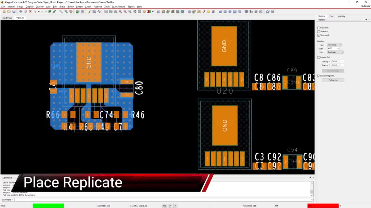
The layout of a power supply circuit showing the close placement of the components.
PCB Placement and Routing Layout Guidelines for Switching Power Supplies
The first step in power supply layout is the correct placement of the components. Power supplies should be spread out across the board so that they are closest to the devices they supply power to. You will also want to consider thermal relief of the power supply components and place them where they will get adequate cooling. The key to reducing the EMI of a switch-mode power supply circuit is to place the components as close together as possible to keep your trace routing short and direct. Start with the main components of the supply first, such as the converter IC, follow that with the input capacitor and inductor, and then the output capacitor. It is also important to keep the parts on the same side of the board to avoid the impedance caused by using vias in the routing.
With the components placed, the next step is to connect the nets together. Here are some routing tips that can help:
-
Following the tight placement of the components, keeping the routing as short and as direct as possible. Shorter traces will lessen the inductance and reduce the amount of noise that could be created.
-
Use trace widths that are large enough to handle the current that is being conducted. The combination of short and wide traces will also help reduce the chance of noise being generated.
-
Use 45-degree corners or round corners in your routing.
-
Avoid the use of vias in your power supply circuitry.
-
Do not route other signal traces through the power supply circuitry.
The final part of the power supply layout is to route in power and ground planes based on the decisions made previously for the board layer stackup configuration. Here are a few key considerations:
-
To achieve better noise control, it is always best to use solid planes instead of routing ground with traces.
-
Make sure that your power supply ground plane is drawn so that it encompasses all of the power supply parts to help with EMI shielding.
-
Separate your power supply ground plane from the common ground of the rest of the design. This will help to isolate the power supply noise from the rest of the design.
-
For power supply grounds that have to connect to the common ground, make sure they only connect at one point to avoid creating antennas that will radiate noise.
-
Do not route digital signals across the power supply ground plane to keep their signal returns from using the isolated ground as a signal return path.
-
To help cool hot power supply parts, use a thermal via under them to dissipate their heat into the isolated ground plane.
With these guidelines, you can reduce a lot of the noise and interference that a switching power supply can generate. Another way you can help yourself is to use the full capabilities of your PCB design tools when laying out the power supplies on your circuit board.
The Constraint Manager in the Allegro PCB Editor showing the organization of power nets.
Leveraging Your PCB Design Tools for Switching Power Supply Layout
We’ve already talked about the merits of using net rules and constraints to set up different routing widths and spaces for your power supply nets. In the picture above, you can see the Constraint Manager within Allegro PCB Editor and how it is organizing the power nets in this design. There are many other useful features in your design tools that can help as well.
Allegro has many different trace routing and copper pour features that will allow you to easily create and edit your power and ground traces and planes. Allegro also has tools such as the IR Drop Analysis Tool that can be used during design to find and correct power integrity issues in your board’s PDN. And, to finalize your design, Allegro’s 3D viewing and checking gives you the ability to see how your design will look before it is built to save you time and money on multiple prototype redesigns.
To find out more about power delivery network design on your next printed circuit board, take a look at this E-book from Cadence.
Leading electronics providers rely on Cadence products to optimize power, space, and energy needs for a wide variety of market applications. To learn more about our innovative solutions, subscribe to our newsletter or our YouTube channel.