Overview of DDR Routing
Key Takeaways
-
The importance of DDR memory routing, and some key points that you should be aware of.
-
From escape routing and terminations to routing and working with HDI designs, these tips will help you with your next DDR memory design.
-
What you need in advanced PCB design tools to get the job done right.

Easily meet timing specifications for your DDR nets with a real-time heads-up display.-
It used to be that computers were thought of as a single object or appliance that served a specific purpose, sort of like plugging in a toaster or a washing machine. Although we know that hasn’t been the case for decades now, most people still don’t understand just how much computing power is actually in use around them every day. All of our smartphones, automotive systems, and IoT devices rely on computing power to get their jobs done, and none of that would happen without the use of DDR memory.
Starting in the late 1990s, the DDR memory standard was developed to provide faster access to data stored in memory. Since its introduction, DDR memory has gone through incremental improvements every 5 years or so to increase its performance and capabilities. While DDR3 and DDR4 are still in use, we are now entering a new standard of performance with the recent introduction of DDR5.
To handle this level of performance, printed circuit boards must be precisely designed and laid out to accommodate the high-speed requirements of DDR memory. Let’s take a more detailed look at what these requirements are, and how you can succeed in the DDR routing on your PCB.
What Is DDR Routing and Why Is It Important?
Computer memory works in conjunction with the processor by sending and receiving signals within the clock cycle of the CPU. Initially, this exchange was done once per clock cycle in what was known as Single Data Rate (SDR) memory configuration. To improve the speed and performance of the data exchange, the signals are now sent and received twice per clock cycle. This Double Data Rate (DDR) memory has replaced SDR and is now the standard of memory configuration.
DDR has been in use for over 20 years now, and during that time it has been regularly updated to increase its speed and performance. The current versions in use are DDR3 and DDR4, with DDR5 having recently become available. Any printed circuit board design that uses memory will most likely employ some version of the DDR memory standard in it. PCB designers need to use precision in their routing of the memory circuitry in order to meet the performance specifications.
Serpentine trace routing for timing signals
Some Key Points in DDR Routing, It’s All About the Timing
The most important thing in routing DDR memory is meeting its timing specifications. The individual signals need to be timed so that the data will be captured on the rising and falling edge of the clock line that it is associated with. Since electrical signals can’t be sped up, the only way to control this timing is to slow them down so that they arrive together at the appropriate moment. This is done by adding length to the traces in a design method known as serpentine routing, which you can see examples of in the picture above.
These specifications have to be met for the memory to function as it is intended to. For PCB designers to hit this timing mark with their routing, it is important that they use the design constraints of their CAD software to help them. These constraints can be set up to work with specific net lengths as well as to route serpentine patterns automatically so traces are routed to their correct length.
As with any high-speed design, however, all of these constraints must be plugged into the entire design parameters of the PCB. For instance, traces routed on the exterior layers of the board will have different timing characteristics than those routed on the internal layers due to their proximity to ground planes. The microstrip configuration of routing on an external layer with only one plane adjacent to it will perform differently than the stripline configuration of inner layer routing that is sandwiched between two planes. All of these factors must be taken into consideration by the PCB designer when planning their DDR routing to achieve the best circuitry performance. As each new version of DDR is introduced, the timing specifications become increasingly tighter requiring even more precision in the routing.
Let’s take a deeper dive now into the specifics of DDR routing. We’ll start first with BGA escape routing and the need for matched terminations in your transmission lines. Then we’ll look at DDR3 and DDR4 routing guidelines as well as general DDR routing techniques and HDI routing in PCB designs.
DDR Routing: Step by Step
DDR memory routing isn’t merely a matter of hooking up traces. The routing must be planned carefully from the initial escape routing all the way through to the end.
Escape routing out of a large BGA package
The First Step Is Designing Your BGA Escape Routing
Routing begins with good placement of components on the board, and DDR memory routing is no exception. Here is a recommended sequence for laying out your components:
-
Fixed components such as connectors
-
Active components (placed for optimized signal paths, cooling considerations, etc.)
-
Outer row of pins on the BGA and routing them away from the part
-
Regular escape routing from interior pins on the BGA (typically dog-bone pattern)
You may find that high-density parts may require the use of via in pads and microvias as well.
This enables you to learn more about BGA escape routing.
Don’t Neglect the Correct Placement and Routing of Your Matched Terminations
Even though your traces may seem to be very short, they will add some delay to your high-speed digital circuit lines, and those delays can introduce reflection problems. If the traces are not terminated correctly, a voltage wave may propagate back down the line to collide with the original signal wave. This may either cancel the original wave or add to it, depending on the polarity of the reflected wave. These problems can happen when the impedance of the line changes in its characteristics due to vias, connectors, and trace stubs. To counter this, series terminations should be added to the line in order to add resistance that is equal to characteristic impedance.
For more information on matched terminations.
DDR3 Routing Guidelines
The DDR3 standard was rolled out in 2007 to replace DDR2, and it is still in use today. A DDR3 DIMM package can have 240 pins on it, which means that there are a lot of high-speed lines that will need to be routed. With that many lines to route, space will be limited and can result in crosstalk, which may cause problems with the signal integrity of the circuitry. As with any DDR routing, the trace length of the critical lines such as data, address, clock, and control signals needs to be tightly controlled for the best performance.
Here are more details on DDR3 routing guidelines.
An example of some differential pair routing
DDR4 Routing Guidelines
Nothing stays the same, but to meet the advancing DDR4 standards, a change in device architecture was required. While DDR3 used a 240 pin DIMM package, DDR4 bumped that pin number up to 288. This led to improvements in its capabilities and speed while at the same time lowering the amount of voltage that was required. It also added more work during PCB design. In addition to adding more critical lines to route, the need for precise place and route techniques increased as well.
Here are more details on DDR4 routing guidelines.
DDR Routing Techniques to Incorporate Into Your Design
To successfully route DDR memory routing, your design must have an optimum component placement, and you must have a routing plan in place. There will be different routing topologies required for the different versions of DDR memory that you need to be aware of. While the T-topology methodology of routing worked great with older versions of DDR memory, it couldn’t handle the higher signaling rates of DDR3 and DDR4. Instead, the fly-by topology gives better success with its daisy chain patterns that also significantly help to improve signal integrity.
If you’d like to learn more about the specifics of DDR routing techniques.
High-Density Interconnects and Considerations for HDI Routing
If you are designing a board with DDR memory routing, you are probably working with a high density interconnect (HDI) design. This means that to be able to squeeze all of the circuitry in, you will be working with more layers on thinner substrates with smaller traces, vias, and pads. When an HDI design is done correctly, you can reap a lot of benefits such as reduced amounts of EMI in addition to creating a smaller board. The trade-off is that a successful HDI design means that more care and attention to detail is required of the PCB designer.
You can find more information on HDI routing here.
Dense routing on a printed circuit board
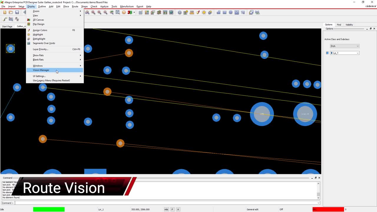
The Right PCB Design Tools for DDR Routing
To successfully route a DDR memory configuration, you need PCB design software that gives you the tools you need for success. Not only does this include creating component footprints and placing those parts on the board, but you also need a fully configurable set of design rules and constraints in order to specify the length and flight times of your DDR signals. Then you need state of the art routing capabilities to put in your traces correctly and at the right length.
PCB design tools like this are already available for advanced DDR routing to keep you ahead of the wave of your competition. Allegro PCB Designer has the capabilities that we’ve been talking about and will get the job done for you.
If you’re looking to learn more about how Cadence has the solution for you, talk to us and our team of experts.