PDN Design for PCBs: A Power Integrity Overview
Don’t fight the power, harness it. This blog will look at the power delivery network and will discuss the following:
- Regulators that generate heat vs. those that generate noise
- Filtering and bypass caps
- Split planes for multiple power supplies
- The role of the ground net for the power distribution network (PDN)
In the world of printed circuit board design, we can classify nets in numerous ways. Normally, the first order of business is about the power domain. Second up is the analog traces followed by the high-speed digital lanes and lastly, the nondescript connections where length and width do not matter as much as any of the above. Here, we’re going to focus on the first item while my other blogs for this month will cover signal integrity for digital and analog routing.
Linear Power Supplies and PCB Layout Considerations
Linear power supplies are the analog version of a power supply. They are well known for stationary locations where power comes from a socket and weight is not an overriding issue. They are designed using large components that dissipate some heat along with transforming the voltage to what will be used around the office including the computer for PCB design.
Coils and transformers make up the bulk of a linear power supply. Diodes create a one way street while capacitors of all sizes stand ready to react to changes in the power. The local powerplant, substation and customers use the same technology, only it’s scaled up for us and our machines.
No matter the scale of operations, the connectivity concerns are based on how much copper is required to complete the voltage transformation down the line. A design rule will force a trace or, more likely, a shape of a minimum width and a maximum length. Short and wide traces are most efficient while sufficient air-gap must also be maintained between different voltage domains.
The rules and construction requirements around a linear power supply makes it a candidate for a stand-alone board. It may be compromised if used on a board with fine-pitch components. Most shapes like to have thick copper plating whereas narrow traces demand thinner copper.

Figure 1. Using a strip of ground along the perimeter of the board on all layers will alleviate emissions from the edges. Image Credit: Author
If the power supply coexists with the electronics, then a wide moat will be required on all layers to help isolate the power supply from the rest of the board. The power plane will cross that divide but that’s the exception. Integrating a 110V or 22V main power source requires a lot of copper pour and also a lot of space. It takes a more involved approach to the constraints to keep the circuit within the detailed design intent of pin-to-pin rules rather than blanketing an entire net.
The Power Integrity Engineer will rightly demand that the constraints are such that the power supply is built right because the design rules will prevent it from being built wrong. Incorporating a route keep-out area under the big inductor may be a step made necessary in order to have the level of control required. Magnetic coupling isn’t contained by a layer of copper so the keep-out regions may affect some or all of the layers.
The SI/PI people have analysis tools on their side. The simulations can predict hot-spots that need relief. The trick is to fix one thing without breaking something else. You might find yourself looking far and wide to any open space you can use.
When you do find an opening, then you have to fill that space and occupy the next space like little dominos until there is a bit of room where you need it. We can take space but we cannot create it. It can be disruptive but we have to shake things up to move a clearing from one part of the board to another.
A power tree has enough branches to have something of importance slip through until we’re close to done. When all of this copper is locked together into a power delivery network, making netlist revision can be tedious. I want to submit the “bones” of the PDN as soon as possible. That way, the EE might find the simple typo on the schematic that’s going to cost me some hours down the road and more hours the further down the road we get.
Component placement has to account for the power grid as one of the primary goals. One layer is rarely enough to untangle the power pins for an SOC. The outer layers can help spread the voltage. First concern is getting to the bypass caps and then getting out of the congested area by whatever means. Most of the power pins are usually located in the center of the chip so bottom side placement of the bypass caps is expected. Proper bypass cap placement is critical. A capacitor too far from its power pin introduces parasitic inductance that undermines its ability to filter noise effectively.
Switch Mode Regulators
When we get to those high pin-count devices, we’re looking at a larger spread of regulators. That brings us to the other type of power supply; the kind that takes in the reference voltage and toggles it on and off in order to generate a spiky current that averages out to the desired voltage.

Figure 2. The bass amp stack runs on switch mode regulators while the PA gear (right) has solid state linear operation. The 2 RU amplifier alone weighs as much as the stack. Image Credit: Author
These devices are known as Switch Mode Power Supplies. The voltage spikes are smoothed out with an LC filter on the V-OUT pin. That means the space between the V-OUT and the inductor has to be short and have low resistance. These circuits come in single gate packages or in multiples using a Power Management Integrated Circuit (PMIC).
The important leg of the PMIC is the V-OUT pins. The inductors that connect to the output pins are too large to get all of the inductors close to their assigned pins. We try to maximize the metal by using a wedge shaped trace that fans out towards the LC filter. The accessible real estate around a PMIC is almost entirely spoken for by the voltage pins.
It’s like there is an anti-gravitational force pushing the power planes away from the center of the device. We want to go from the outer layers to inner plane layers with a cluster of vias. The clusters are spread out to allow bus routing on some layers and voltage planes on others.
We wind up with concentric rings of power around SOCs that cluster power pins near the center of the pin field and out towards the corners. Expect a few virtual iterations while the power integrity people analyze the PDN.
The copper planes for the power domain should adhere to the 6H rule. That’s what it was called the first time I’d heard about it. The idea is that the voltage plane should be inside the board outline by a factor of six relative to the thickness of the dielectric material used for the individual layers of the stack-up.
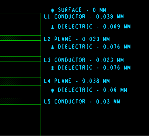
Figure 3. This stack-up has layer 4 as a plane layer sandwiched between dielectrics that are 0.076 and 0.060 in nominal thickness. Using the larger value, a keep-in area for the PDN would be (0.076 mm x 6) = 0.456 mm from the board edge.
A common printed circuit board with through-hole vias will be the hardest to fan-out, especially for BGA packages, since every via blocks routing on all layers. High density interconnect mitigates density challenges and replaces them with cost and schedule hurdles. The smaller vias give up a lot of cross section compared to a plated through-hole via (PTHV).
Even though we stack the microvias, they do not form as cohesive of a thermal path as the PTHV. The best thing we can do for the inner layers is to tie them to outer layers using whatever vias the design supports. A good power domain requires an elastic approach.