Printed Circuit Board Design for Manufacturing
The qualifications to get a job in printed circuit board design are a far cry from what it took when I entered the workforce. If you could decipher a schematic and knew how to use the ECAD tools, you were in. Not so today. I have a deep admiration for many of my readers who are schooled in advanced mathematics and even physics in order to hold down a job. Even entry-level candidates are expected to hit the ground running.
In this article, I will discuss the following:
- Design For Manufacturing principles
- Stack-up strategies that align with product goals
- Fabrication notes that keep the wheels turning
- Ways to retain lessons learned along the was
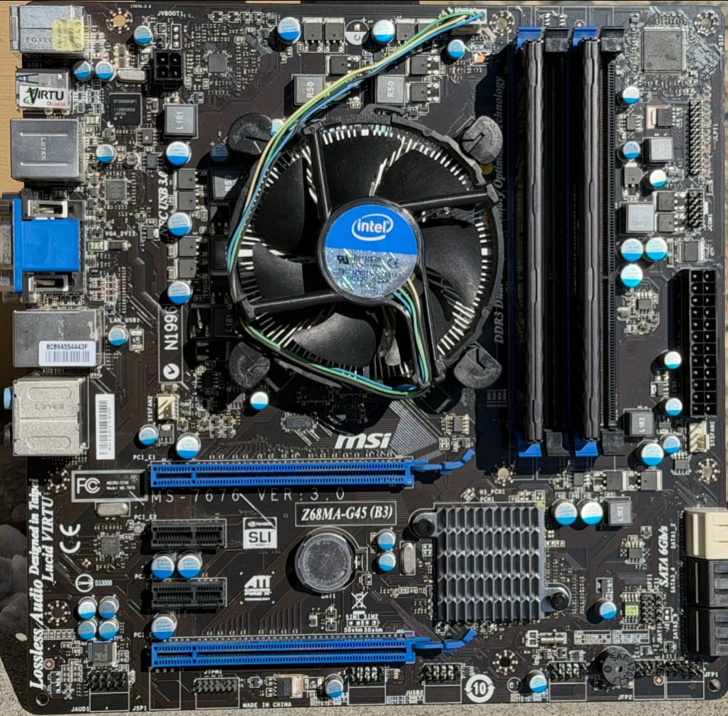
Figure 1. The nearest I’ve come to designing a board like this is an edge router with four processors. Add a memory controller that drives four solder-down memory modules plus four expansion slots. Ten identical ethernet ports rounded the connector scheme. The power integrity was assured by copious design rules. Image Credit: Author
Component Vendors Have Their Best Interest In Mind When Providing a Reference Design
When we want to get a PCB design off on the right foot, it usually starts with browsing through app-notes and diagrams that show a chip in isolation on a large bring-up board. Every eventuality is covered from the dielectric material to the tolerances on critical dimensions. The component will shine under these conditions.
The thing is that we rarely have the luxury of all of that space for dedicated supporting circuits while maintaining absolute isolation. More functionality equals more devices and more competition for limited space. Almost everyone wants the printed circuit board to be smaller and lighter without sacrificing performance. That can be a tough nut to crack. This is one of the issues with reference designs.
The Component Mix Will Determine the PCB Geometry
I’m reminded of a combo-chip that incorporated WiFi, Bluetooth and an FM radio receiver packed into a WLCSP. I wrote about this device a few years ago under the title Wafer Level Chip Scale Packaging: What is That? The takeaway from that effort is that you have to think small and accept the higher price and longer lead time involved with High Density Interconnect technology. That decision is basically forced on us designers by the device geometry.
From a philosophical standpoint, I would rather that the fabricator have a challenging task rather than sending a sub-par bare board into assembly. By that point we’re further down the timeline and have invested in all of the components. So, while this story is about making artwork that works at the fab-shop, we’re ultimately responsible for the product as a whole. Part selection at the schematic stage will ultimately define the PCB technology.
Our job is to do the best we can with the space available. Obviously, the path to gaining space for cleaner routing is to add layers to the board. This drives up the cost of raw materials and fabrication processes so we can’t get away with over-provisioning the stack-up.
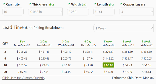
Figure 2. Time is money but technology is also a factor. This is the first part of a list of parameters that will drive cost where lead time is the biggest expense. An automated order form like this allows us to do what-if analysis before committing to a specific technology. Image Credit: Sunstone Circuits
Bigger PCB Geometry is Better For Fabrication
Our default is to use plated though-hole technology for the PCB. Typical low tech boards go from two to four layers with a single lamination cycle. Using an even number of layers is key to a manufacturable board. Keeping trace and space geometry above 100 microns (4 mil) on outer layers and 76 microns on inner layers allows almost any fab shop to quote and fabricate our boards in less than a week.
“Do not let mechanical or electrical engineers push you to request a tighter thickness tolerance.”
Asking the vendor to create a stack-up is a reasonable request. They need to know if you have controlled impedance. You need to provide the PCB thickness target allowing for a +/-10% tolerance. Do not let mechanical or electrical engineers push you to request a tighter thickness tolerance. It’s just not going to happen with a multi-layer board. If they insist that you must specify it their way, then they will find out that you are right which will help your credibility in the long run.
Being generous with each parameter leads to a more robust board with lower cost. Green soldermask is old-school and is the best value. I use 8-mil via hole finished size for most boards but larger ones will reduce cost. A 13-mil via is going to be more producible and better at handling power demands. That seems to be the point of diminishing returns.
Larger capture pads will be more manufacturable but the cost is paid in terms of the impedance discontinuity. It’s a balancing act between DFM and performance. The IPC classification will determine the proper annular ring for plated holes. The class will determine the reliability which will be determined by the environment and use case of the end product. Going into orbit requires more space; pun intended.
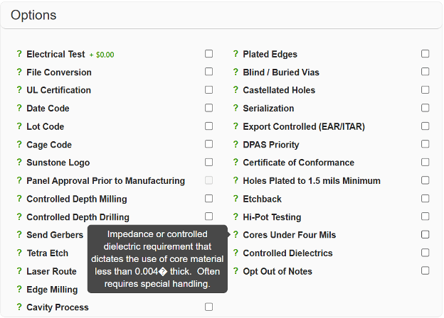
Figure 3. Skipping past the lengthy basic information window takes us to the options where the more you select, the more you pay. The question marks create a pop-out that provides more detail when you hover over one. Select your cost-drivers carefully. Image Credit: Sunstone Circuits
Giving the factory a detailed list of requirements cuts down on the number of technical questions that hold up the board from going into fabrication. You start with a dimensioned outline, a stack-up diagram, and an impedance table that provides linewidth and spacing per layer as appropriate. The main thing beyond that is the fabrication notes.
Fabrication Notes: A Brief Set of Attributes That Can Be Assured Through Inspection
Fab notes can clarify what is not covered by calling out the IPC specs. In some cases, it helps to point out what is already covered but don’t take it too far. I’ve listed some common notes below although your requirements may vary. It is traditional to use all-caps so that’s what’s next.
NOTES: UNLESS OTHERWISE SPECIFIED
- INTERPRET DIMENSIONS AND TOLERANCES IN ACCORDANCE WITH ASME Y14.5M.
- FABRICATE IN ACCORDANCE WITH IPC-6012 CLASS 2
- DO NOT SCALE DRAWING
- MATERIAL: FR4 (Tg180) HALOGEN FREE IAW IPC-4101/21 OR EQUIVALENT
- SURFACE FINISH: ENIG IAW IPC-4552
- HOLE PLATING SHALL BE MINIMUM OF 1 MIL THICKNESS, VOIDS NOT TO EXCEED 20% OF DIAMETER. HOLE SIZE MEASURED AFTER PLATING
- SOLDERMASK OVER BARE COPPER IAW IPC-SM-840. COLOR: GREEN
- SILKSCREEN SHALL BE WHITE NON-CONDUCTIVE INK. REMOVE ANY INK OVER EXPOSED COPPER. VENDOR LOGO, DATE CODE AND UL MARKING TO BE ADDED WHERE SHOWN
- ONE SOLDER SAMPLE AFTER LEAD-FREE PROCESS TO BE INCLUDED WITH EACH ORDER.
- ELECTRICAL TEST IAW IPC-9252 USING PROVIDED IPC-365 NETLIST.
The more you ask for in the notes, the longer it takes for the vendor to digest the tape-out. Then the boards arrive, and everything has to be inspected in accordance with those notes. Knowing what is covered by note 2 goes a long way towards streamlining the output.
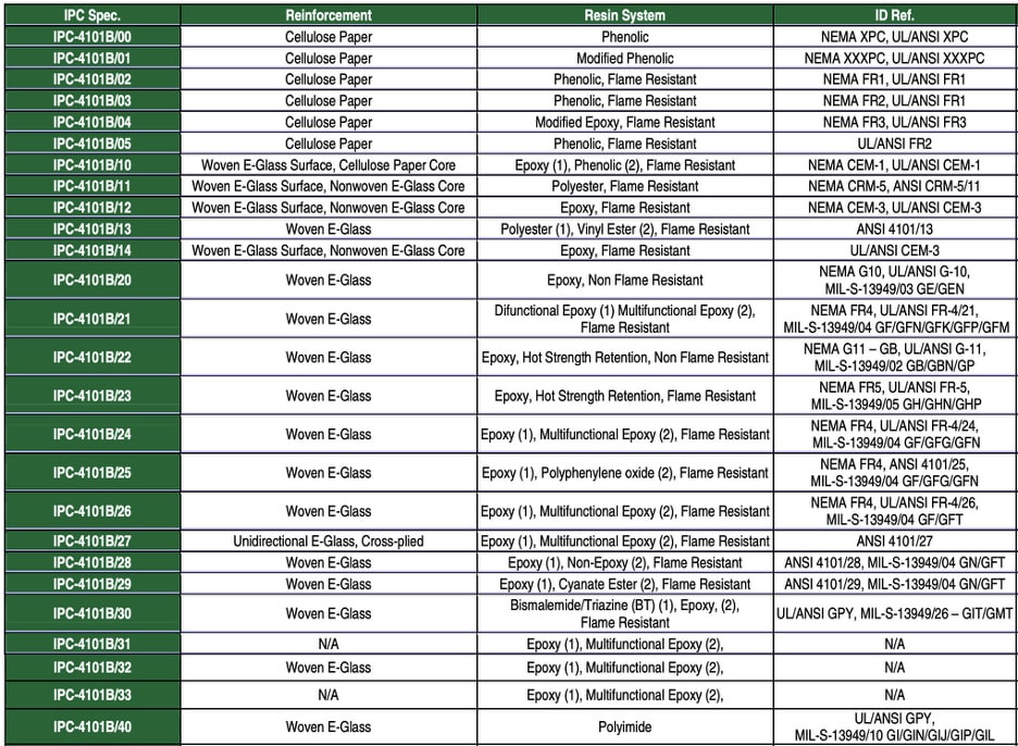
Figure 4. This is a partial list of slash sheets from IPC-4101B which is obsolete, while Rev E is current. This still shows the flavor of how slash sheets are documented. There are other columns for things like the dielectric constant and the all-important temperature rating. Image Credit: Standard Printed Circuits
Something like the copper thickness in the barrel of the hole is likely to be challenged by the CAM department. Plating the holes also plates up the outer layers. That’s why trace and space geometry is greater for the top and bottom layers than the internal layers.
By the time the board is released to production, the barrel plating may be down to half of what’s specified. If you see the same technical questions from multiple sources or the same source again and again, it’s a good idea to incorporate those limitations on the next iteration of the board. The SI/PI people may have an ideal outcome that may not match the reality on the ground.
When I tape out the first revision and get feedback from the vendor, I’m going to begin a Rev. 2 that accounts for their show-stoppers. That database will be kept local and noted as an as-built file. That way, when a routine iteration occurs, the DFM list of questions is shorter or, hopefully, nonexistent.
It can be very useful to create a log for reference. That way, you will be able to disclose the changes that were made outside of whatever Rev. 2 puts on your plate. Most engineers are averse to arbitrary and capricious changes other than their own bug fixes. Having a clear justification for what you did will smooth out that path to success. I’m going to run with this DFx theme over the coming months. If this interests you, then watch this space for more.