PCB WEST 2025 - The Show Must Go On
Four days of learning and meeting like-minded people in the PCB design arena.
PCB West has come and gone once again. The mid-week Expo was jammed with vendors and customers. The bread around that filling was four days of presentations from leading experts in their fields. The first thing on the agenda was the PCEA (Printed Circuit Engineering Association) annual meeting chaired by Stephen V. Chavez. He got us pumped up for the rest of the show. Steph and Mike Buetow were both given well deserved awards to round out that meeting.
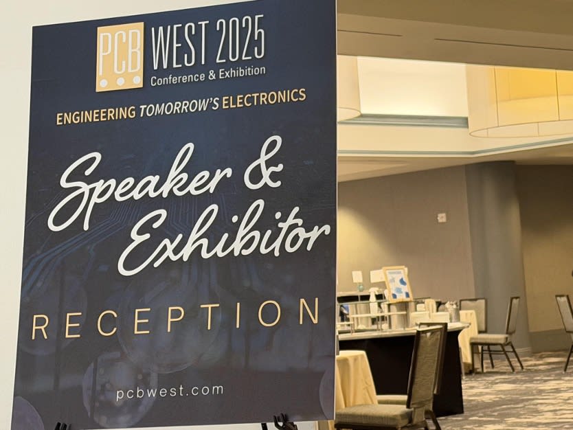
Figure 1. The Hyatt Regency and the Santa Clara Convention Center once again hosted PCB WEST 2025.
Day 1: The Learning Sessions Begin
From there, I sat in with Troy Hopkins for a long discussion about stack-ups. This is fundamental to PCBs and spills over into mechanical and electrical aspects of the boards. As with other talks, there was space in between for the attendees to chat among themselves. There was this blue haired, baby faced gentleman named Justin Flemming sitting back there with me who had really impressive knowledge that you would notice by the nature of his questions and comments.
I asked him how he became so knowledgeable in this field. His answer was that he invested in himself through the purchase of many IPC documents, lots of research and study to know the intricacies of fabrication and assembly. Impressive.
The next name I want to drop is Juan C. Frias. He is a new speaker and worked his way through a slide deck, walking us through the finer points of fabrication and assembly drawings. Juan has a long record of treating me like a long lost friend. He's always happy to see me and the feeling is mutual. These three activities made up the first day.
Day 2: The Expo
Everything is amplified when the crowd shows up. The sessions continued throughout so it was time to join the Rick Hartley school of "energy flows between the copper layers". Actually, it was one of his Deans, Dan Beeker, carrying the torch. I like his passion even when he's saying that I underestimate the speed of light. Wait, what?
In addition to the smaller break-out rooms, there was a big theatre where, among other things, was the keynote address about rainmaking and a panel discussion called "Training the PCB Designer/Engineer of the Future". Both were interesting topics while the theatre provided a cool place to take a breather.
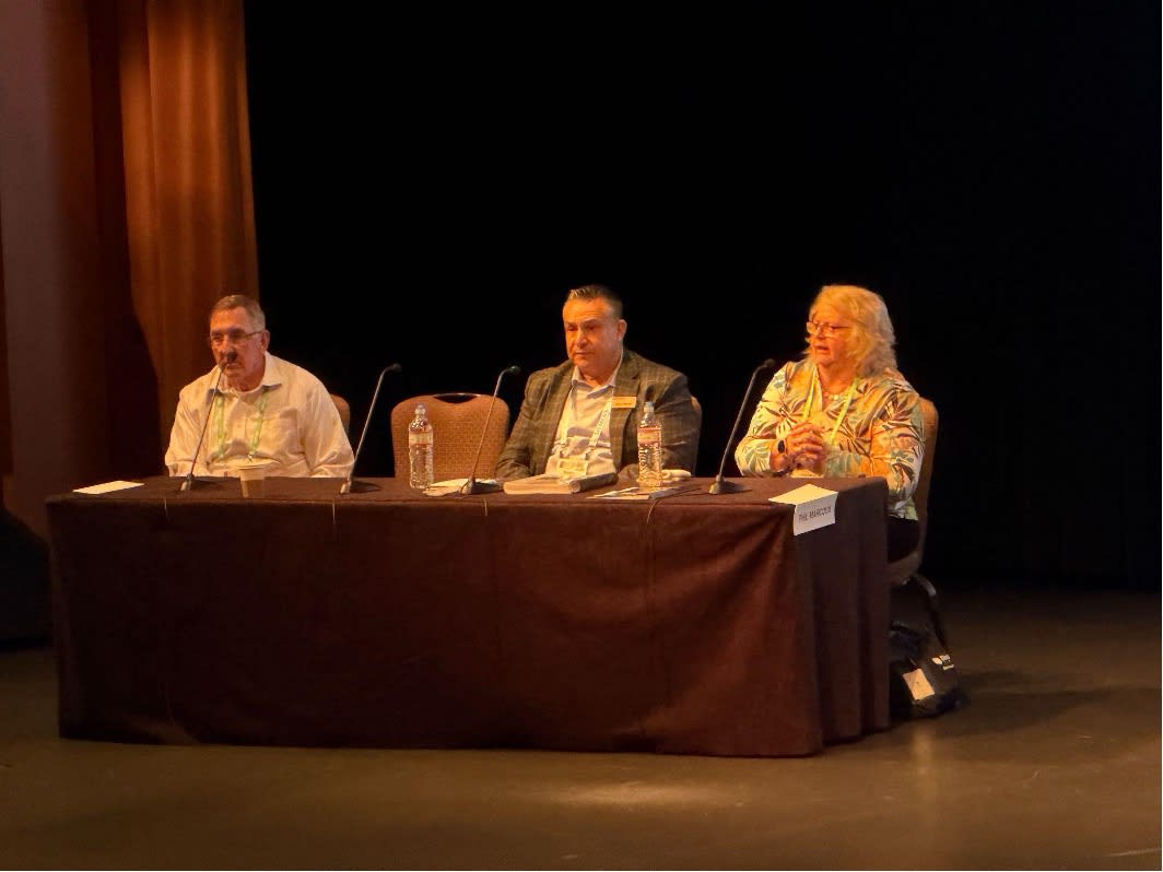
Figure 2. The three person panel of experts giving guidance to the up and coming PCB Designers. The moderator was none other than Mike Buetow who organized the conference. Image Credit: Author
After the lunch break, I felt like joining the crowd for the expo. Again, my hosts at EMA Design Automation had the first booth as you walked in. As usual, their next door neighbor was Cadence with Siemens right across the hall. Sierra Circuits also occupied that row making it one in which to spend some time. It was like big names in the center with smaller outfits along the flanks.
When it was all over, the organizers shifted over to a reception hour. Snacks and drinks were served and the atmosphere perked up for the final hour. I drank a tequila sunrise out of a ziplock bag. Thanks EMA! Some cheese cubes and bread were all I needed to finish off the evening. I will circle back to the sessions but first let me try to explain how to make the most of your limited time with so many different vendors at the exposition.
How To Prepare To Make The Most of the Expo
Out of all of the conventions I've been to, this was the first time I was able to attend the full affair. I've always been able to make the most of the gathered vendors with this one bit of preparation. In the weeks leading up to the event, I'm surveying the landscape in the office and looking for shortcomings in our knowledge or pain points in our process. There is always something we have to improve.
An example of this is when I was designing printed circuit boards for Lidar sensors. The inventor of the technology and founder of the company did his own PCB layouts. While he is a genius, he's not adept at creating cost effective PC boards; a little too creative.
We ended up with some radical technology where we join several tiny boards to a larger one without any connectors. The little boards had lasers or detectors that fit into special slots in the larger boards. They were held together with a solder bead kind of like grout between the kitchen counter and the backsplash. In order to pull this off, the plating was only 50 microns from the edge on all of the boards.
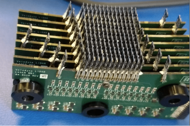
Figure 3. This image shows 128 little boards attached to a total of 8 bigger boards. The method of connectorless connections involves placing the laser boards into the slot orthogonal to the carrier boards. The dabs of adhesive are applied after the lasers have been aligned using special equipment on a 60 meter, indoor range.
There is an ODM vendor that specializes in optical circuits including lasers who could do this work for us. The vendor was Fabrinet and we didn't have a second source. So, I went to every PCB vendor in the expo hall asking them about their minimum gap between the edge of the board and the copper. We were using lasers to create board outlines for more lasers. The larger boards that held the lasers and detectors were also laser defined. This was due to the intricacies of the slots that held the little boards.
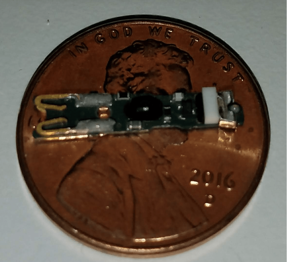
Figure 4. This PCBA is highly engineered for its size. It is depaneled using a laser to form the outline. Here and on the larger boards, the copper to edge specification is down to 50 micrometers (two mils). The component-to-board edge situation is also suspect.
There were 128 lasers and 128 detectors in total; each on its own little PCB. It took 8 different boards to shoot the photons out and 8 more to detect the reflections. That's already 272 printed circuit boards. We still had the round logic board and another "donut" for the motor that spins all the lasers and detectors.
Is it any wonder that these things cost 10s of thousands of dollars? Anyway, PCB West from about six years back was my chance to take the pulse in terms of plating near the edge. For the record, the leading edge of metal pullback was 127 micrometers at that time.
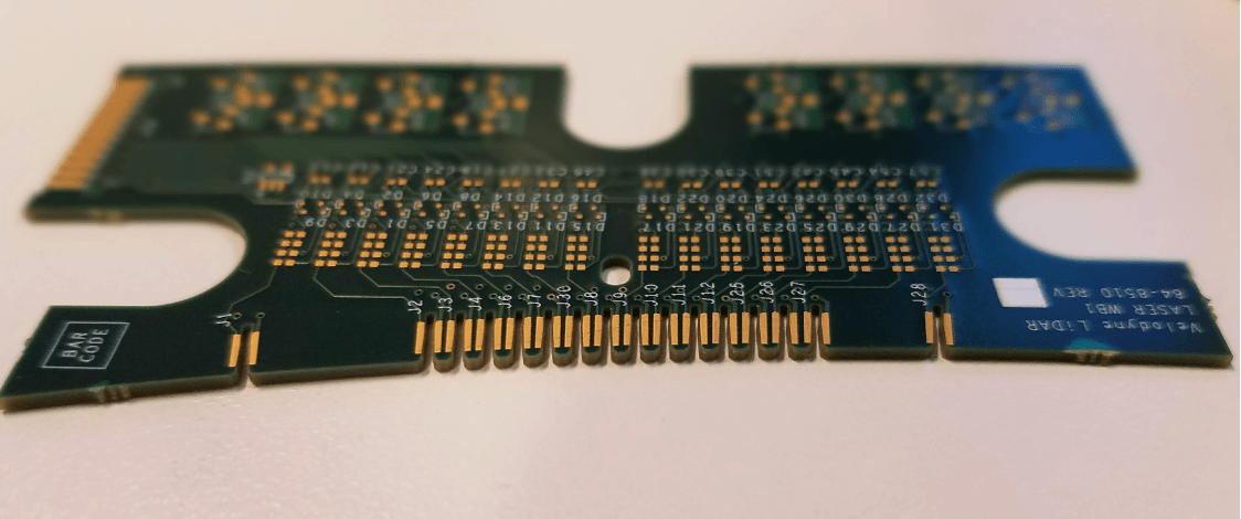
Figure 5. The octet of boards that hold the lasers and detectors have this one edge on the outline that cannot be produced with regular machining technology. The laser cut slots are shown along the lower edge. The negative space between the pins has an almost imperceptible hourglass shape. The pins look like they are plated clear to the edge although the artwork pulls back by the 2 mils mentioned above.
Another time, I walked through the Expo with a full size blueprint with a list of notes that included very tight layer-to-layer registration requirements among other things. Every time I spread out the blueprint, the people at the booth went into DFM mode, giving me guidance on how to facilitate the misregistration limits. Every PCB convention had me looking for such a cause to explore.
Day 3: The Learning Sessions Retake Center Stage
We're back to the slide shows and the quiet comfort after the high energy expo. The first stop was with Rick Hartley himself. He delivered a full expansion of mixed signal design. This is tantamount to a full spectrum essay as mixed signal has a foot in the analog and digital streams.
I'm here to say that Rick is ready and able to dress down the EE's when it comes to doing things his way. I only have a fraction of the backbone and contempt for the schematic drawing egg heads. I'd take his advice but advise implementing it with a more amenable demeanor. Securing a second opinion in your favor takes a little back-channel work but it really helps credibility.
The third day was finished off with a lesson from Zachariah Peterson. He taught us about signal integrity while implementing UHDI technology. It's a lot of theory - and math. I understood most of it though I was hoping for more insight into the practical points and pitfalls of moving to UHDI.
As it turns out, Thursday is the traditional supper out at a local Mexican restaurant that caters to the expense account set. The 11 speakers who took part treated me as one of their own. It's like Rick Hartley knows me by name and reads my column! On that note, I'd like to thank you for reading mine.
Day 4: An Easy Transition Back to Normal Life
People come from around the country to speak at PCB WEST. They need to catch a flight home to their families for the weekend. Thus Friday starts a little later and ends a little earlier than usual. That gave me time for two more solid seminars. The morning had me in with Keven Coates. He talked about DFA and DFM with regards to first pass success.
Another "lunch and learn" was sandwiched between that and the final period. I'm ending up right where I started four days prior with Stephen Chavez. He was giving us the lowdown on DFM in terms of UHDI. Overall, the show looked like a success to me. If you want to share your knowledge there is an option to submit an abstract and become a speaker. If your paper is chosen, you could be the one to boost the next generation of PCB designers.