Home
Free Trial
Home
Free Trial
Read More
Content
Filter
10 results found
Featured
PCB Power Integrity Analysis: Why PDN Behavior Is a Geometry Problem
Featured
Why Rule-Based Signal Integrity Checks Miss EMC Issues
Featured
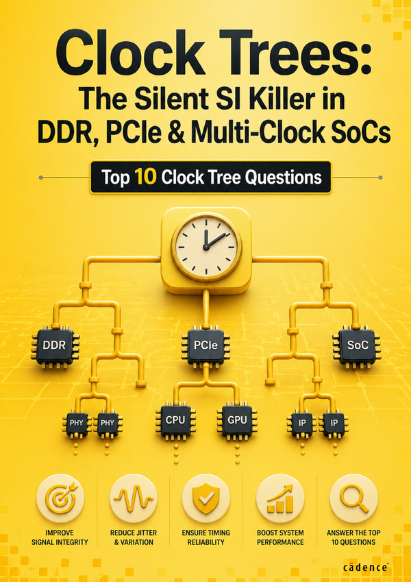
Top 10 Clock Tree Questions
Featured
RF PCB Layout: Transmission Lines, Impedance, and PDN Design
Featured
PDN Design for PCBs: A Power Integrity Overview
Featured
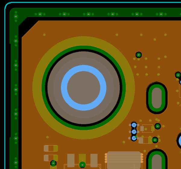
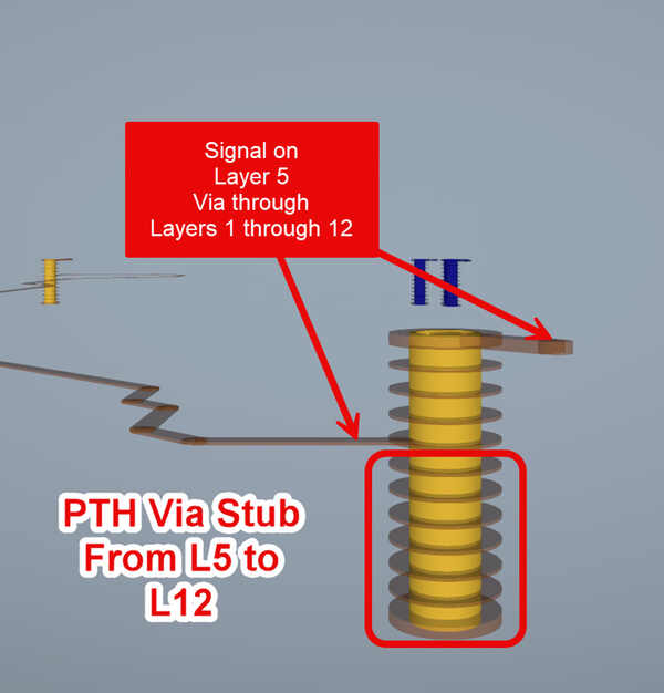
The Hidden Cost of Via Choices in High-Speed Designs
Featured
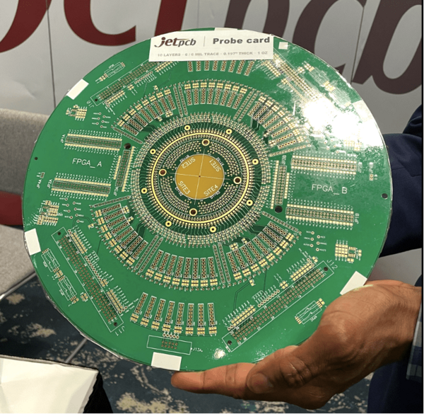
Testing Printed Circuit Boards and Assemblies
Featured
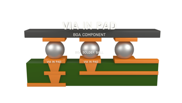
Why Decoupling Capacitor Placement Becomes Harder in HDI PCB Designs
Featured
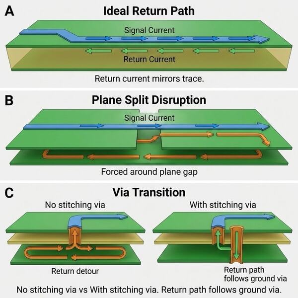
When Do Layout Decisions Become SI Problems?
Featured
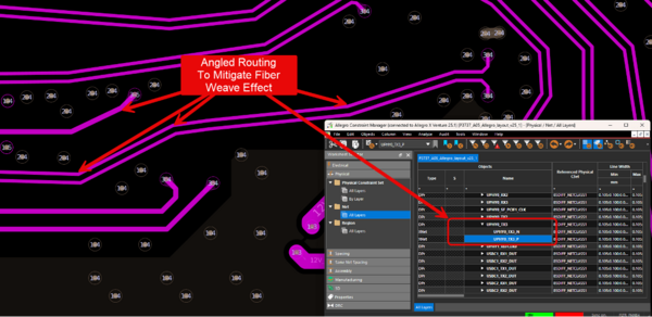
The Physics of Resin Flow: Glass Weave Locking & Dielectric Behavior in HDI Laminations
Featured
Products
None
Allegro X PCB
(1)
Content types
None
Blog
(9)
Technical Documents
(1)
Solutions
None
PCB Layout
(9)
Simulation & Analysis
(4)
Constraint Management
(1)