PCB Design Strategies: High-Density Interconnect (HDI) Techniques
HDI Placement and Routing
Printed Circuit Board design involves a lot of editing of previous circuits. Then there are times when the board is an empty polygon waiting for you to populate all of the virtual symbols. This is followed by connecting them with the graphical version of the traces and shapes. All of this effort creates a digital twin of the product. PCB Designers have figured out that connecting the dots is a small part of the day-to-day saga of product development.
The PCB Designer's task is to create that above mentioned twin based on a number of competing factors including:
● Meeting DFx requirements within IPC specifications for the class
● Capturing design intent as rules driven constraints for validation
● Reserving the space required for FCC immunity
● Thermal performance/battery life
● Ever-decreasing form factors
● Progressively shorter timelines
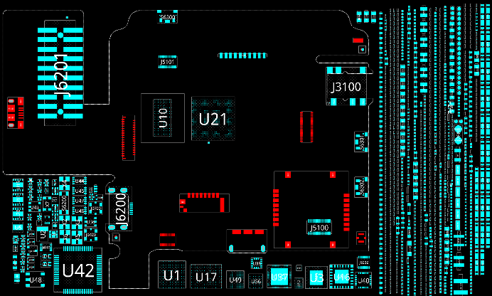
Figure 1. Step one of the placement study is to see if all of the parts are in the library. The components that are already placed were largely predetermined by the outline drawing. It gives confidence that we can place the board but there will be parts on both sides. Note that the outline drawing requires double sided component placement to begin with. That gives us a lot more real estate. The critical check will be for how much headroom can be had on the far side. There are often keep-out areas reserved for cables and other features. Image Credit: Author
The pressure is on from day-one. To gamify the process, there are elements of chess, jigsaw puzzles, Tetris, connect-the-dots, SimCity and even Grand Theft Auto where you have to take space from one thing to provide for something else. Different interests can have you feeling a bit like King Solomon wondering how to divide up the finite space on the board during the even more finite schedule.
Size Matters: The Smaller, the Better
There are things we can control and things we can only hope to influence. Asking for more room half way through hits differently than when you make the case right away. New boards feature new connectors and other items that need to bubble up through the library to the layout.
"Clean that up before making copies all over…"
If that's your job, build them to the best of your ability to aid such things as organizing silkscreen. The "Wizard" will build errors into the library footprint. Creating zero-width silkscreen over pads is one of them. Clean that up before making copies all over the board. If routing under a certain kind of part is a problem, solve it at the component level with a route keep-out. A little extra work on the library pays dividends.
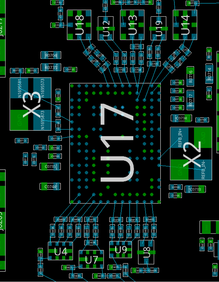
Figure 2. This is a classic example of the connections driving the placement. Matching networks, switches and diplexers are among the ancillary components that find their way into an analog block. The placement details favor the flow of the traces more than the assembly house's preference for consistent component orientation. The shortest trace is the best trace. Image Credit: Author
When it comes to placement, it would be natural to start with the parts like connectors where the location is already determined. If there are ESD suppression diodes involved, it's a no-brainer to get them close to the connector pins. Not everything is so simple to discern but there can be clues on the schematic. Setting up automatic cross-probing is pretty easy.
Once you do that, every part you click on in the layout tool is shown on the schematic. After you've used cross-probing that way, it's going to be in play for all of your placement and power delivery decisions. I feel like I have a hand tied behind my back without it. Sometimes, an engineer will leave local notes on the schematic with instructions. That's just one more reason to look for context when placing components.
The chip maker wants you to adhere to the diagram or assume the risk …
Of course, another thing that is nice to have is a quick link to the data sheet for the various chips. App notes will provide placement diagrams for optimal performance. The chip maker wants you to adhere to the diagram or assume the risk when/if the device fails.
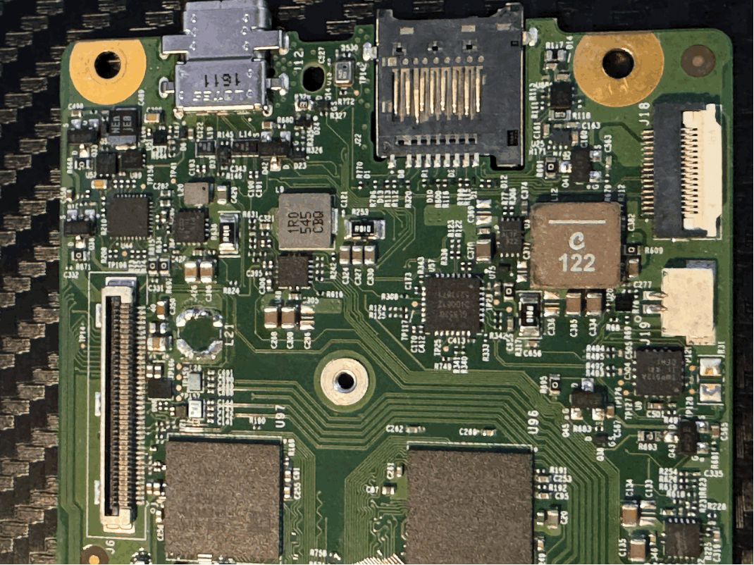
Figure 3. HDI PCBs support the microelectronics common in today's computers and other electronic devices. The thickness of the bare board is 1 mm saving some space in the z-axis. We like thin computers with lots of batteries. This holds true for almost everything. Image Credit: Author
Do it their way or you're on your own. In reality, you have more parts than the diagram shows plus the data sheet may include hole tolerance call-outs that are beyond the capacity of the fabricator. When it comes to devices that are layout dependent, placement will be negotiated as those little parts get shuffled around to squeeze into the limited space.
If there is no existing work to copy, I like to create an ideal layout for a device outside of the board outline before putting the whole thing on the board. The little parts often reveal the full context of the routing.
Other than that, placement is about walking down the schematic page picking symbols and having that part's footprint appear under my cursor in the layout tool. Again, using the cross probing to do a placement or using the highlight command to colorize a page worth of components keeps things in focus. That will be handy if you've already run a quick place to see what you're working with on a page by page basis.
With the biggest chip stuck in the middle and the connectors out on the edge, all that's left is the smaller groups clustered around the board outline in their rainbow of highlight colors. Of course, the memory is going right next to the processor chip. There are some obvious choices like that and there's the grey area where it would be nice to have it close to the device. Count on having more ancillary devices than "storefront" around the primary devices.
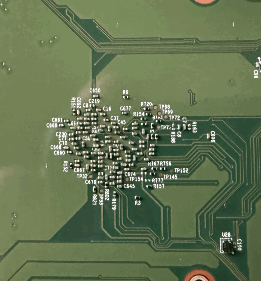
Figure 4. A cluster of 0201(imperial) caps and resistors plus a few test points support a processor on the opposite side of the board. Silkscreen was omitted from many of the components as there wasn't sufficient room. Image Credit: Author
The bottom of the board is often the best side for the application of bypass caps. They're small and they are numerous. When a chip is 10 mm or more across, the bottom side could get much closer to the inner grid where power and ground pins are fairly common. The inductive loop will be measurably shorter. This is especially good for those capacitors that are measured in pico-farads, like 22 or 47pF for example.
Big bulk caps can use the top side and do their thing at a distance. There's lumped capacitance and then there's distributed elements. We have those and usually some ferrite beads to split up the power domains. It's common to start with lots of filters and capacitors then try to depopulate certain ones to see if they are really needed. We can't take anything off of the board until we fill it up.
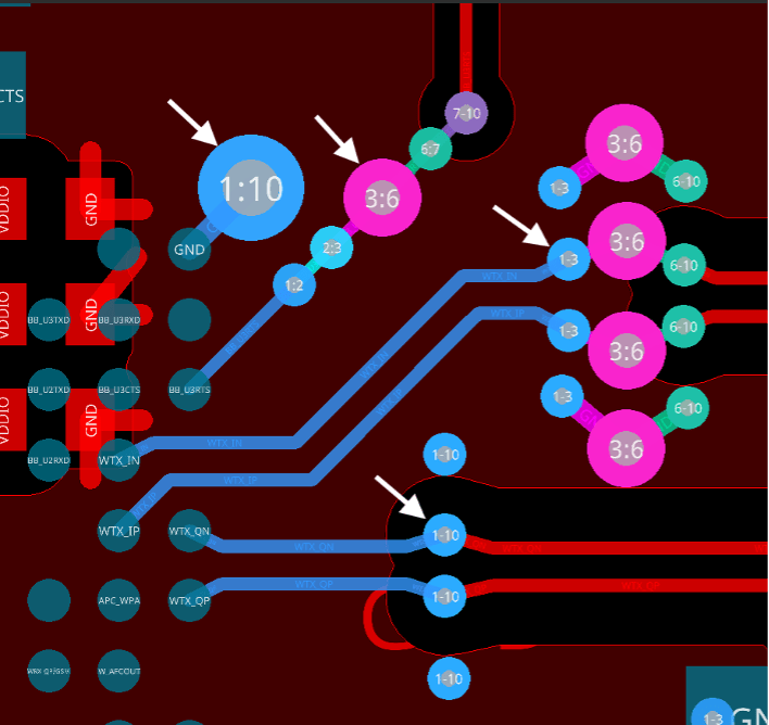
Figure 5. The component placement spacing will be influenced by the routing topology. Around the horn we have a plated through-hole via followed by staggered microvias with a buried via then over to the diff-pairs using stacked micro vias with buried vias and finally a full stack of microvias.This fan-out study also proves that the copper pour rules that give extra space to the differential pairs. Image Credit: Author
The advantages of High Density Interconnect Printed Circuit Boards:
● No additional space is required for fan-out by using via-in-pad technology. Minimum component spacing is generally sufficient all around.
● The smaller microvias are lower in impedance and that helps with signal integrity.
● Back-drilling is unnecessary as the via can go from one layer to any other layer with the exception of buried vias.
● HDI boards may be the only option with many of the leading edge devices on the market. The fine pitch parts are usually the first package out of the gate for new silicon.
The process of creating HDI boards requires more than the traditional single lamination cycle. Each sequential layer pair takes the same amount of time to laminate as a complete through-hole board. The press is both expensive to buy and is the bottleneck in the typical fab shop. The result is a higher cost for labor and a longer lead time for High Definition Interconnect circuit boards. As they say, you pay to play.
Read Part Three Here: Optimizing Mixed Signal Circuit Designs