Concerning Thermal Challenges With Printed Circuit Boards
It has been said that good things come in small packages. This is true of electronics up to a point. Chip companies are competing for bragging rights on package size. Less is more. Increased density allows faster operation as there is less lag in the shorter traces. It's not just the chips that are seeing this trend. Making the whole product smaller is a marketing breakthrough.
Meanwhile, a compact board will have more wattage to dissipate per unit area. The power supplies are spread around the board with dedicated regulators assigned to each chip even when the voltage requirements are the same from one device to another.
Linear Power Supplies Vs. Switch Mode Power Supplies (SMPS)
Traditional linear power supplies are not as efficient as switch mode power supplies. The difference is that the linear power supplies create much more heat than the SMPS devices. That heat doesn't just materialize out of nothing. Power is wasted to create the hot spot.
Switch Mode power supplies avoid this problem but create a different issue. The tradeoff is that the SMPS circuits generate considerable noise that has to be managed with a large LC filter. While the linear power supply produces continuous power at a given voltage, the "switch mode" toggles the full input power on and off to come up with an average power that is sufficient for the device under load.
We use the filter to smooth the SMPS output voltage out so that the device behaves according to the app notes. The placement and routing of the filter and other components is a key factor in the performance of the power supply. Most mobile devices will use this technology.
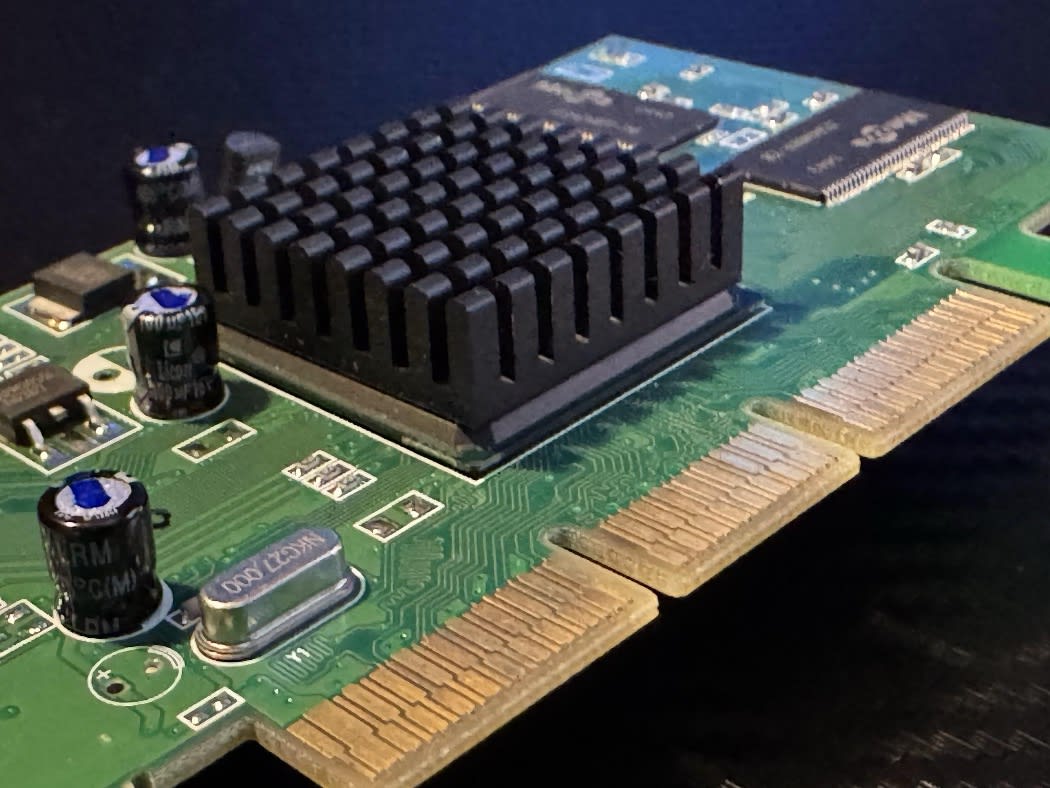
Figure 1. A graphics accelerator card or GPU uses a heatsink with pin fins for dissipating the thermal load. Note the left edge of the image shows two D-PAK (TO-252) components which are linear regulators. They get warm on their own but avoid the potential noise concern of a switch mode power supply. Since this GPU is ultimately plugged into the wall socket, efficiency isn't as important as a lower noise floor. Image Credit: Author
Heavy Copper - A Means to Turn The Whole PC Board Into a Heat Sink
As part of the Chrome OS Hardware team, I was tasked with the layout of two boards intended to test different laptop batteries. They were big boards that held several batteries each. Beyond the natural heat of operation, the boards were placed in a type of oven known as a burn-in chamber. It's a carefully regulated hot box that included a pen that charted the temperature over time on a scroll of graph paper. This would serve as proof of the environmental conditions of the test.
A bunch of batteries running near maximum rated output in a torture chamber that would cycle the temperature up and down would require a robust board. I went with 4 ounce copper on the outer layers and three ounce copper on the two inner layers. The vias were huge relative to the normal ones. I also designed an aluminum frame to go under the board which would stiffen it against the weight of all of the batteries while also acting as a heat spreader.
Some batteries would not make it through the test. Those "infant failures" would be analyzed. While the cells were off-the-shelf items, the battery packs themselves were bespoke units. We needed to know if it was the cells or the construction that led to failure. That's why the PCB fixture was over-designed. I took the total expected dissipation of the cells and did 100% derating. If we needed to deal with 45 watts, the design goal was to accommodate 90 watts per battery.
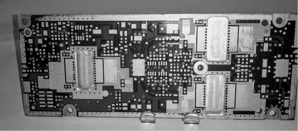
Figure 2. This is a board that the fabricator, Sanmina, used in their trade show display. What's remarkable is that the bottom (Layer 4) is a solid plate of copper. Two dielectric layers of GTEK separated the three other layers. High temperature rated materials and 45 oz copper across the entire bottom gave this amplifier the robustness required to drive signals from cellular base stations to phones within the cell. No fewer than five meetings preceded the tape-out. Image Credit: Author
Active Cooling: When Passive Efforts Fall Short
Moving air is a good thing. When it happens naturally, we use a term called wind-chill to factor in the cooling effects beyond the ambient temperature. Internal combustion vehicles will normally feature a radiator with coolant flowing through it while a fan and the vehicle's movement augment the flow of air through the fins of the radiator.
The same thing plays out on a printed circuit board. Cooling fins will be attached to the high wattage devices and a small fan can help evacuate the lingering heat. This prolongs the lifespan of the device and allows it to keep running while crunching the numbers. There are these really thin blowers that can be incorporated in the z-stack of our laptops to keep them from going into thermal shut-down. It's typical to cut out the board around it so it can be mid-mounted to reduce the impact on the overall thickness of the machine.
Graphic heavy programs like Allegro X Venture can cause the fan to come on just by opening a sufficiently large design. Running something like the Power Delivery Solution Generator or other automation is sure to tax the system. Given a choice, I'd prefer a tower computer to a laptop for this reason. The air-flow is better, the heat sources are more spread out and there's room for more active cooling. My gamer laptop works for ECAD but I can hear it struggling right away.
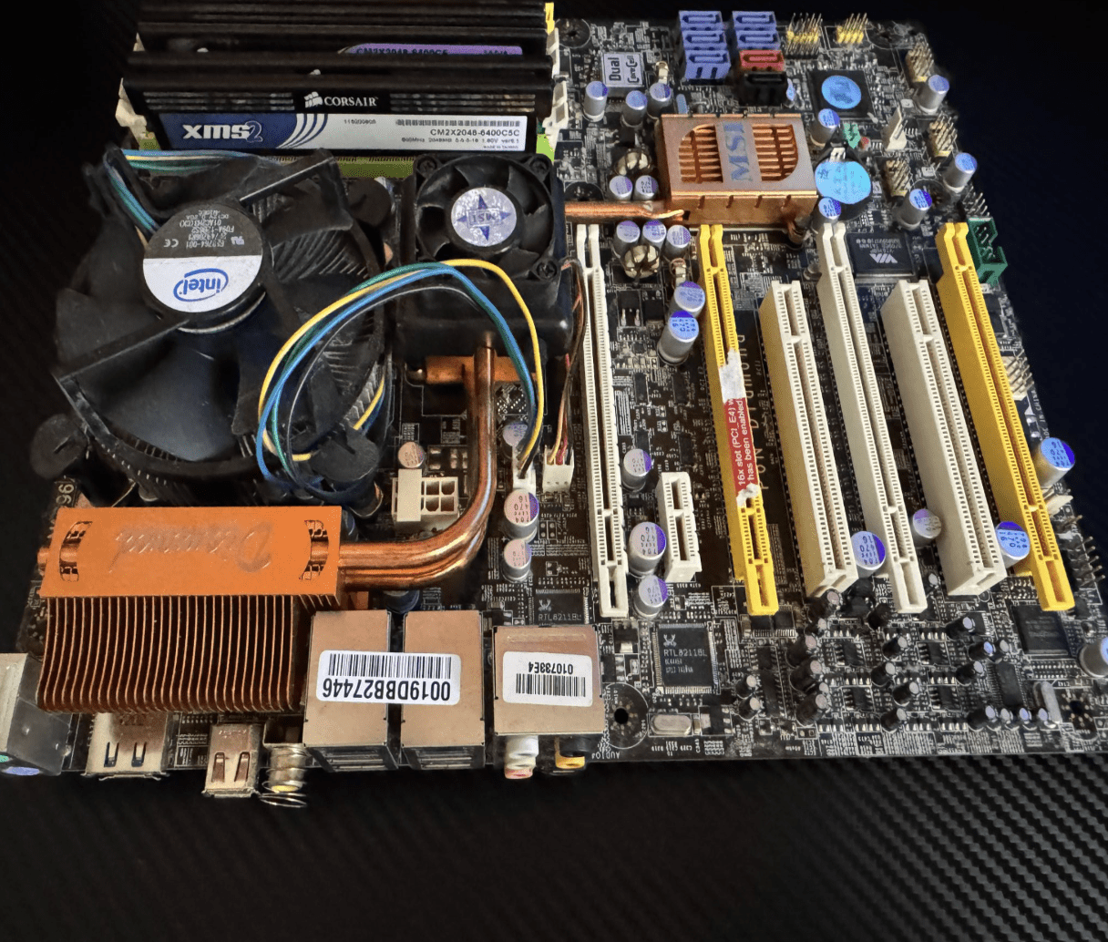
Figure 3. Active cooling methods include the fan over the heat sink over the SOC. Furthermore, heatpipes can be implemented to pull the heat towards a radiator located away from the hot spot(s). This is from an old "gamer" computer where graphics are a priority. Image Credit: Author
Wrapping Up The Discussion on Thermal Challenges
Success in thermal management includes paying attention to the ground paddles that underpin the QFN/QFP packages with perimeter pins and a big central pad that is grounded. We're constrained by space to put vias in the big pad. Micro-vias are naturally better even if they are not rated to dissipate as much wattage as a full plated through-hole via. The soldering process is less of a risk with micro-vias. Plated though hole vias would want to be plugged with a solder mask or filled with thermally conductive material for best results. An open via hole is an invitation for solder to creep away from where it's required under the flatpack device.
The specific methods will vary depending on the application and, of course, the chipset itself. The form factor will determine the available solutions. It could involve the use of graphene or other exotic materials that can be used to extract thermal energy from the system. As parts and systems shrink, we're tasked with ever increasing current density. We need to consider thermal management during floor planning so that there's space between hot spots.
Even though a connector doesn't create heat on its own, it may be underprovisioned in terms of number and size of the pins to carry the current. Breather holes in the chassis and other efforts may be considered in the service of thermal management. Derating of components can prolong the mean time between failures. A well planned layout will include considerations for thermal management. Aim for higher reliability for lower on-going cost related to field service or warrantee claims. It all starts with keeping your cool.