Metaphors for PCB Layout
Life is more fun if you have a vivid imagination. The jargon we use in PCB design comes from regular words where we’ve expanded the definition. I see no harm in expanding things a bit more as required. They used to be called ‘Mother Boards’ but the Chromebook team called them Main Logic Boards or just MLBs. Back when it was still cool to bristle with connectivity we had our share of I\O ports.
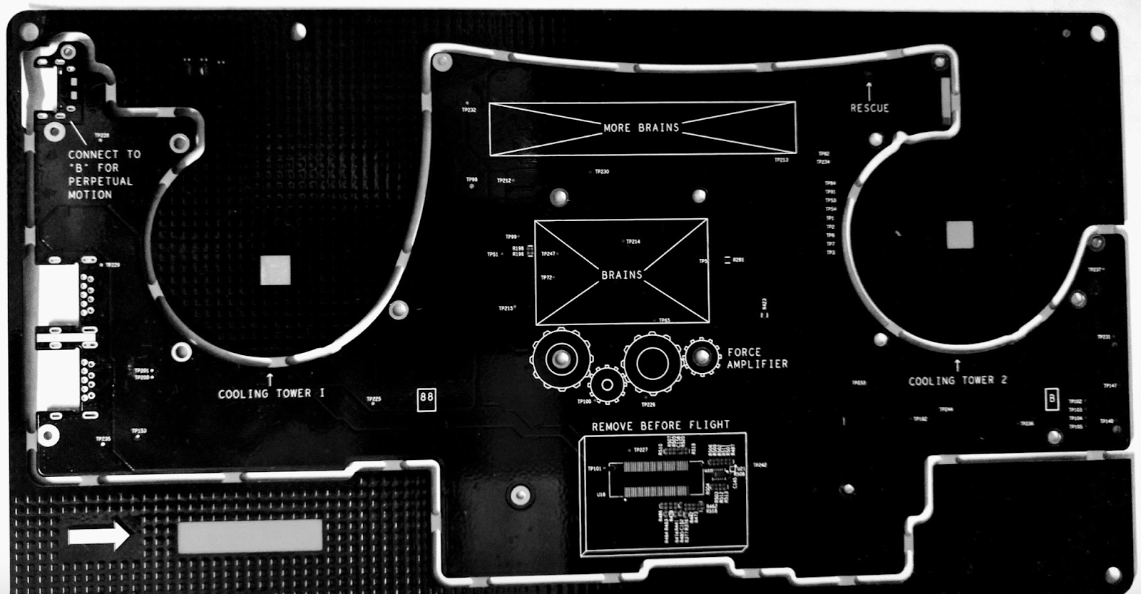
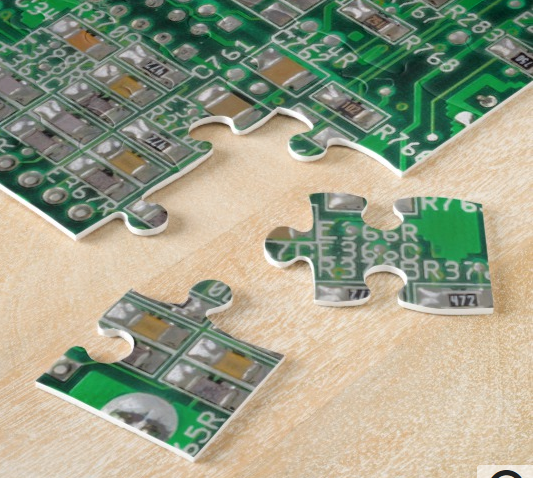
Image credit: Author - MLB with some novelty silkscreen
The Pixel laptop MLB of the day had a roughly rectangular outline with a pair of notable cut-outs for fans. Though it looked nothing like a map of the United States, I named most of the electronics for the city they would cover if laid over the map. The USB 2 connectors were along the lower left and became San Francisco and Los Angeles. USB 3 was above in Seattle. There was another one on a flex out in Atlanta, NFC was in New York and GPS lived in Miami. All the chips had a home town. I hope I’m not the only board designer that is keen on geography.
The simplest board can stand in for a room, you know, a light, a fan, a speaker, something like that. Little boxes can grow to a household or small apartment building. Just add a microcontroller and get your Maker hat on. As I’m positioning these parts, it’s like arranging furniture. Get enough furniture and it takes on the likeness of a Sim City. Nobody has ever called me a gamer but I did enjoy a few months of building a virtual town without raising taxes too much. Good times. Board design as civic planning. Yep.
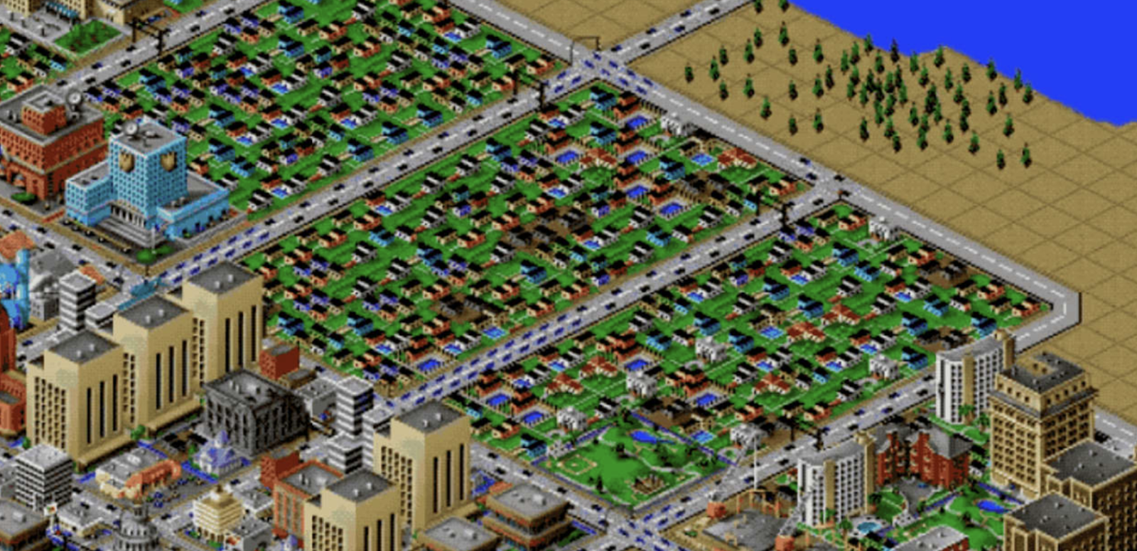
Image credit: EA games
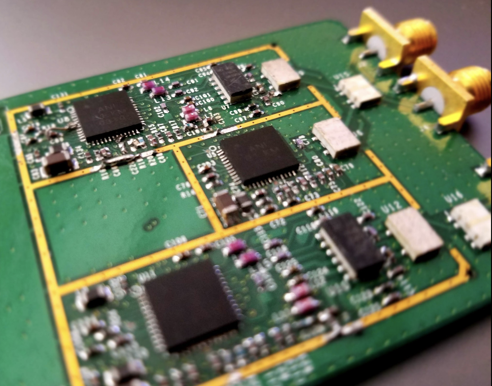
Image credit: Author
One-Trick Ponies
Purpose built boards are mostly one-trick ponies because they don’t like to share space with other ponies. Most of your radios and power modules are like that. Typical sensors are analogous to their organic counterpart. That is cameras, microphones, and speakers are akin to eyes, ears, and voices. Throw in some artificial smarts and these organs start to show some signs of life. Add in the ability to propel itself around and we’ve got some kind of mechanical pet. Scale that up and add a pleasant interior and we’re doing level 5 self-driving!
Adding a super-power for safety in the event that someone actually builds self-driving shuttles (they did) and have people ride them (they do), is my job. The superpower, of course, is the Lidar sensors; 360-degree perception is a neat feature. Autonomous bots that walk, float, fly, ride or drive become more common with each passing year. There is a lot of work to do to bring it all together. Interesting times.
So, we’re not just playing Tetris (placement) or connect-the-dots (routing) those are just side benefits. All of the component footprints take on the character determined by their function. It is what it does. It can also be whatever we like to think of it as. It’s your crystal, it’s my barn or heart. It’s your connector, it’s my toll plaza. That’s not a thermal sensor, it’s my feelings. Don’t hurt them by trying to pull me back to your reality. Oh, go ahead, reality is necessary at times.
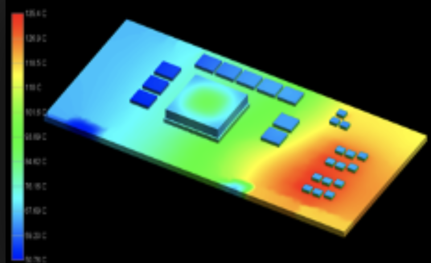
Image credit: Cadence
The truth is that PCB design involves a wide number of factors that will require judicious balance. Have you worked with full feature system on chip (SOC)? With a lot of devices, we cannot provide the preferred amount of copper for our voltage planes. There are just too many of them.
We cut corners and juggle the minimum size shape to meet the requirements by a hair. It is a tug-of-war between the different voltage domains. They all want their share of what’s available on the layers allocated for power - and any routing layers you can use to stitch things together. Submitting your best guess to the PDN team for simulation is sort of like rolling the dice in a game of Risk.
Image credit: Ben Stephenson / Flickr
Your feedback will consist of a plot of where the hot spots demand a little more room for this or that power domain. You carve a little away from one shape to add more to another. Reroute a perfectly good trace so that it makes way for the Balkanized power set-up. Submit another virtual iteration. Roll the dice again when they recheck the current density.
Simulating is so much cheaper and faster than spinning out actual physical PCB iterations. SI/PI functions will veer off into their separate graphics. I mentioned the heat map and we also have the other side of the design, signal routing. That’s where we can see an eye-diagram.
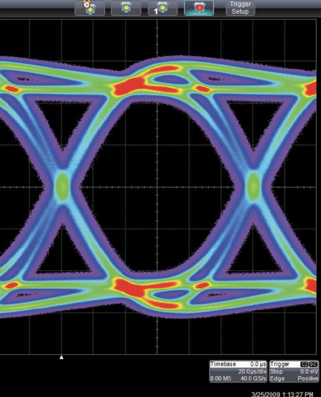
Image credit :EE Stack Exchange
Look into my eye. Tell me what you see. Some overshoot but it’s consistent so, good eye.
The product could also take on a wireless aspect. Cut the cord and you have Smith charts, the ultimate Rorschach test.
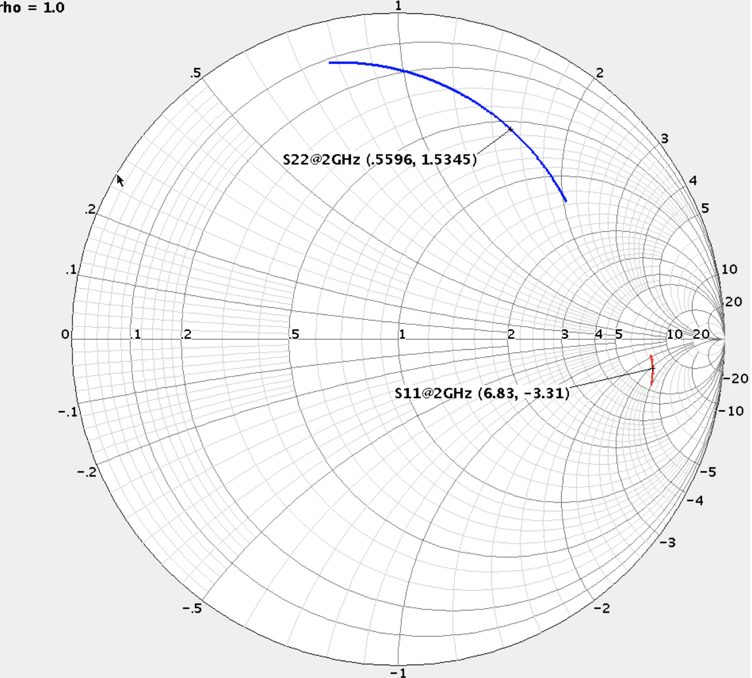
Image credit: Cadence
Who would even think of drawing this graph, let alone make sense of the curves? Of course, lots of analog engineers are intimately familiar with the zones of the chart. For the rest of us, it’s just a guess. So, we can always substitute our own reality for the mysteries around us. We can think of other parallels in nature and beyond for the functions we bring into being. Visions or railroad tracks or superhighways scale down to miniature versions of themselves to connect the hives of activity on our printed circuit worlds.