BGA Fanout Techniques for Efficient PCB Design
Key Takeaways
- BGA fanout techniques assist in managing signal integrity, thermal performance, and manufacturability in high-performance PCB designs.
- Choosing the right method, like dog bone, via-in-pad, or microvias, depends on BGA pitch, routing density, and design complexity.
- Advanced PCB design tools like OrCAD X make BGA fanout easy with automated fanout generation, impedance control, and built-in design rule checks.
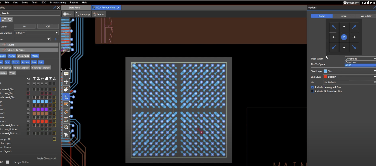
Fanout your BGA, as well as set constraints, in OrCAD X
A PCB designer must navigate the complex landscape of Ball Grid Array (BGA) fanout with precision and foresight. The challenge? To create a reliable and efficient pathway for signals to escape the dense pin field of a BGA package. When you're staring at a high pin-count BGA, the task of routing all those signals can feel like an overwhelming puzzle. But with a methodical approach and the right BGA fanout techniques, it’s a puzzle you can solve.
BGA fanout refers to the method of routing electrical connections from the BGA's ball terminals to the traces on the printed circuit board (PCB). Because the BGA pins are tucked away under the chip, special techniques are needed to make reliable connections. It's not just about connecting the dots; it's about ensuring signal integrity, managing thermal performance, and optimizing manufacturability.
Considerations for BGA Fanout Design
The BGA fanout is important to PCB design, especially with integrated circuits featuring high pin counts. A well-designed fanout can improve signal quality by reducing signal reflections and crosstalk. Effective BGA fanout maximizes routing efficiency, minimizes signal degradation, and allows you to meet the performance requirements of modern electronic systems. Furthermore, it can simplify the soldering process, leading to higher production efficiency and lower costs.
Several factors come into play when designing a BGA fanout:
- Pad Design and Spacing: The pads that connect to the BGA balls must be positioned precisely with sufficient spacing to prevent short circuits and ensure reliable solder joints.
- Via Types and Placement: The choice of via type – whether plated-through, blind, or buried – significantly impacts routing density and signal integrity.
- Conductor Routing: Traces must be routed to avoid crossings and maintain adequate spacing to prevent shorts.
- Signal and Power Integrity: Minimizing signal reflections and crosstalk is vital, particularly for high-speed signals. Power supply paths must be designed to deliver sufficient current without causing excessive voltage drop or noise.
- Thermal Management: A well-designed fanout can aid in heat dissipation, preventing component overheating and extending service life.
- Layer Stackup: The arrangement of layers in the PCB stackup greatly affects routing capabilities and signal integrity. Controlled impedance layers and dedicated signal layers can enhance routing efficiency.

Some examples of BGA escape routing patterns on a PCB design system
Common BGA Fanout Techniques
As BGA technology has evolved, so have the fanout techniques. Here are some of the most common:
|
Technique |
Description |
Pitch Suitability |
|
Dog Bone Fanout |
Uses short traces ("dog bones") to connect BGA pads to nearby vias. Simple and cost-effective; suitable when space allows routing between pads. |
Not suitable for fine-pitch; best for larger-pitch BGAs |
|
Via-in-Pad |
Vias are placed directly within BGA pads; they require filling and plating. Enables the highest routing density. |
Suitable for fine-pitch BGAs only |
|
Via-near-Pad |
Vias are placed adjacent to pads; this avoids via-in-pad complexity while maintaining good density. |
Suitable for most BGAs |
|
Stacked and Staggered Microvias |
Uses laser-drilled microvias (stacked or staggered) for high-density interconnects. Ideal for multi-layer HDI designs. |
Best for fine-pitch BGAs and high-density layouts |
|
Routing Between Pins |
Traces are routed directly between BGA pads to escape to the outer layers. Effective only when sufficient spacing exists. |
Not suitable for fine-pitch; good for larger-pitch BGAs |
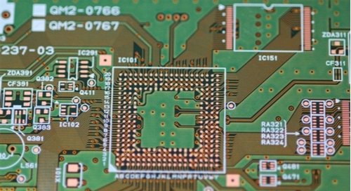
Careful planning goes into routing out of a BGA package like this
Selecting the right fanout strategy involves a combination of factors, so remember some tips for making your design successful:
|
Tips for: |
Description |
|
BGA Pitch and Density |
The BGA’s pitch dictates the complexity of the fanout. Smaller pitches reduce the space available for trace routing. |
|
Layer Stackup |
Plan for a suitable layer stackup that supports signal integrity and routing efficiency. Use controlled impedance layers and consider adding routing layers for higher-density BGAs. Tools like Sierra Circuits’ Stackup Designer can assist. |
|
Design Rule Checks (DRC) |
Use DRC features in tools like OrCAD X to detect issues such as clearance violations and trace width errors early in the design. This ensures compliance with both industry and custom requirements. |
|
Signal Integrity |
Maintain signal quality through impedance matching, short stub lengths, and proper via placement. Essential for high-speed signals to avoid reflections and crosstalk. |
|
Thermal Management |
Use thermal vias and optimize airflow to dissipate heat from high-pin-count BGAs. Proper thermal design extends component lifespan and ensures reliability. |
How OrCAD X Aids in Applying BGA Fanout Techniques
Modern PCB design tools like Cadence OrCAD X offer a range of features to simplify BGA fanout:
- Automated Fanout: Automatically generate fanout patterns based on design rules and component parameters.
- Rules-Driven Routing: Define design rules for trace widths, clearances, and via sizes, and let the software enforce those rules during routing.
- Impedance Control: Calculate and maintain controlled impedance for high-speed signals.
- 3D Visualization: Visualize the BGA fanout in 3D to identify potential clearance issues or manufacturing problems.
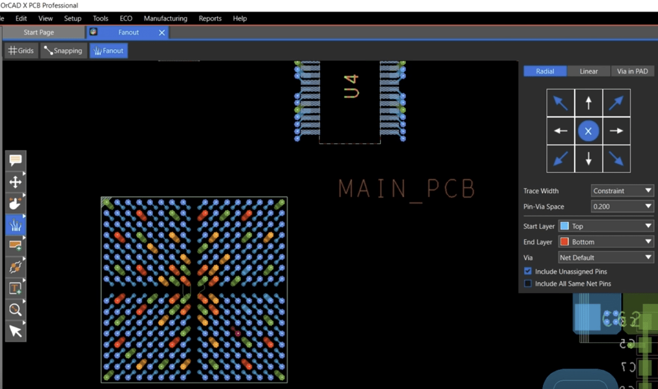
Easily fan out entire components with a click in OrCAD X
Proper utilization of BGA fanout techniques is necessary to escape the dense pin jungle of modern BGA packages. With Cadence’s powerful OrCAD X platform, you can automate fanout creation, maintain impedance control, and collaborate directly with manufacturers. Don’t let BGA complexity stall your design—take advantage of high-speed rule setups, 3D visualization, and real-time DRCs to ensure signal integrity and manufacturability. Start your free trial of OrCAD X and explore the full platform here.
Leading electronics providers rely on Cadence products to optimize power, space, and energy needs for a wide variety of market applications. To learn more about our innovative solutions, subscribe to our newsletter or our YouTube channel.