PCB Layout of Chips On Board - Skip the Package and Join the Fun
Substrates are used as a carrier for the silicon. The two main reasons are to avoid a CTE mismatch and to protect the integrated circuit from the environment. Another benefit is that the connections can be spread out so that a lower technology PCB can be used. Some types of packaging will have a lead time measured in months. They also cost a lot of money in non-recurring engineering (NRE) and a bit more per piece. There are cases where it makes more sense to lose the transposer and put the device right on the PCB. Let’s take a look at that idea.
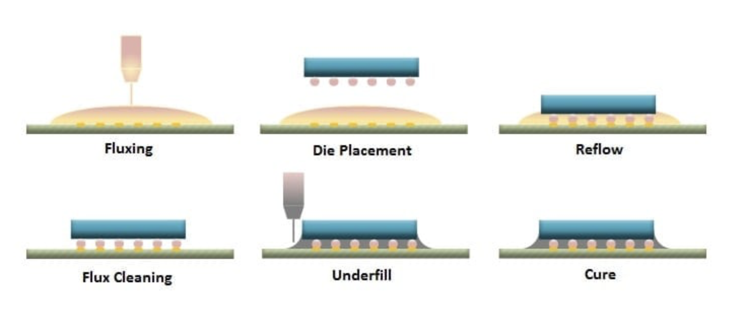
Chip-On-Board (COB) is just what it says on the tin. There are basically two ways to perform die-attach. One way involves bumps on the bottom of the die; just like a normal BGA except smaller. These “Flip Chips” will test your PCB vendors ability to create tiny footprints. Then they will test your assembly partner’s ability to place, reflow and underfill the Flip Chip On Board (FCOB).
The underfill is necessary because of the different coefficient of thermal expansion of the materials. Without the underfill, the CTE mismatch will stress the flip chip to the point where the connections will not be reliable.
The other method is to have a solid metal base that is bonded to the substrate with epoxy or solder. The connections are on the top of the die in the form of rectangular openings in the passivation layer that covers the rest of the IC. Wirebonds are used to make the connections from the passivation openings to pads on the host material. It’s this second type that is the best candidate for COB assembly.
In standard production of this type, there is usually a die cavity that sets the chip down in a recess so that the top of the die is closer to level with the surface that will have the wirebond pads. The wirebond pads are typically oblong in shape There may even be a mezzanine, known as a stepped wirebond cage. COB will more likely keep everything on the same surface which makes for slightly longer wire bonds.
The PCB will require a selective plating of soft gold for the wirebond pads. This will limit the types of finish used elsewhere on the board. Instead of ENIG or OSP, it may be better to use ENEPIG which adds a layer of palladium to the finish.
There are two basic types of wirebonds; ball bonding and wedge bonding. They both use the same type of non-stranded wire; typically made of aluminum or gold. Copper is also used but non-insulated copper and normal air are a bad mix. Ball bonding attaches the end of the wire to the device using the tip of the wire for the connection. Wedge bonding lays the wire flat on its side for the connections. That method is used on the board side of the connection.
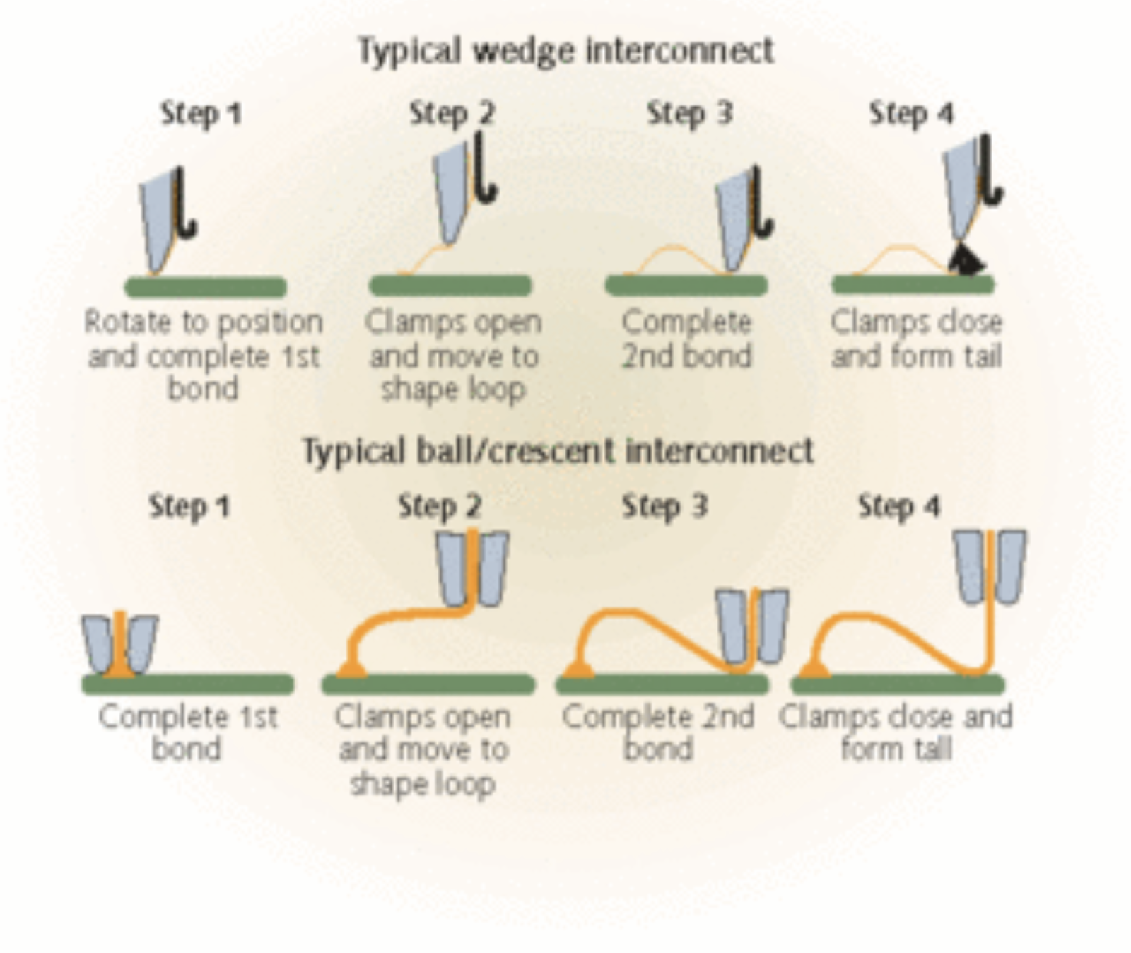
Image Credit: Semiconductor Digest - Ball bonding is more popular since the machines can do them faster.
The trade-off between the two types is two-fold; loop height and launch angle. Ball bonds have a slightly higher loop height but can have a wider launch angle of up to 45 degrees from the die. Wedge bonding has a lower profile but the bigger contact area reduces the launch angle to around 30 degrees.
The wire is typically 25 microns in diameter. An upper limit for the length of the wire is 100 times the diameter. These parameters will be critical in determining exactly how the wirebond cage is formed. Depending on the device, you could have between one and four concentric rings around the die. Skipping a wire or reassigning it to a different pad allows us to modify the behavior of a chip during development.
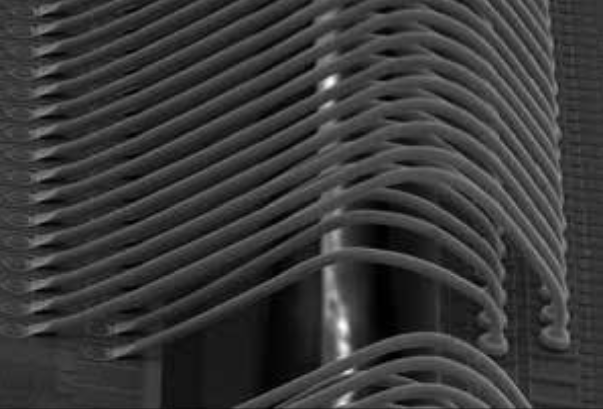
Image Credit: Semiconductor Digest - two rows of ball-bonded wires with the chip on the right-hand side.
Note that most assembly shops will have to outsource the wirebond process even if they can attach the chip to the board themselves. Automated wirebond machines are expensive. I recall a vendor asking for a .dxf file so they could program the machine. Small ICs as well as LEDs and Lasers are among the candidates. Chip companies and larger factories may keep this in house.
So, you have the die attached to the PCB and wires connecting the die to the board. Now what? Start with an initial test of the PCB assembly. If all is well, then the factory can add a glop top to the COB. Potting the whole affair in a non-conductive epoxy material will protect the delicate wires from being pushed into one another and may allow some thermal dissipation. In a regular device, the die is sealed inside the package so there is little need for a filler material. It will be simpler to rework a traditional package than an encapsulated chip on the board.
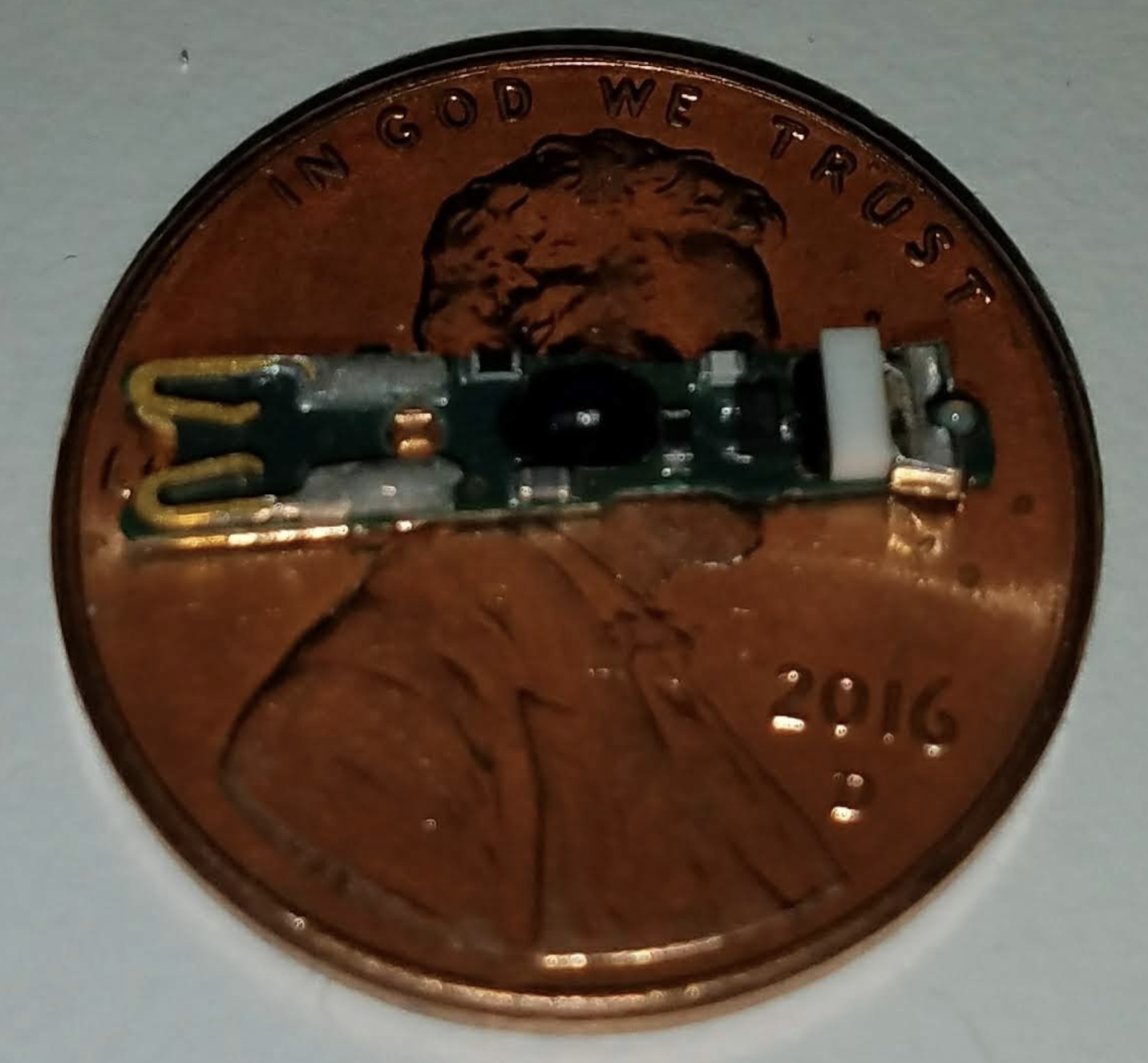
Image Credit: Author - Some PCBs are just too small for a regular package
Taking the three processes into account, die attach, wirebond and encapsulation, COB still weighs less, has a lower profile and a smaller footprint than a Ball Grid Array or Quad Flat Package component. The cost and development time may be reduced while reliability is on par when using Chip On Board technology. So if your project is feeling the squeeze, get on board. I’ll bring the chips.