How CAD and CAM Work Together
Computer-Aided Design (CAD) refers to the entire body of work around the product. Printed Circuit Board CAD design focuses on the layout of virtual components and their connections on the PCB. This subset relies on a specific type of Computer-Aided Manufacturing performed by CAM Engineers who are typically employed by PCB fabrication shops. PCB CAD layout people end their job by creating electronic files that the CAM operator uses to generate the photo tools for the PCB.
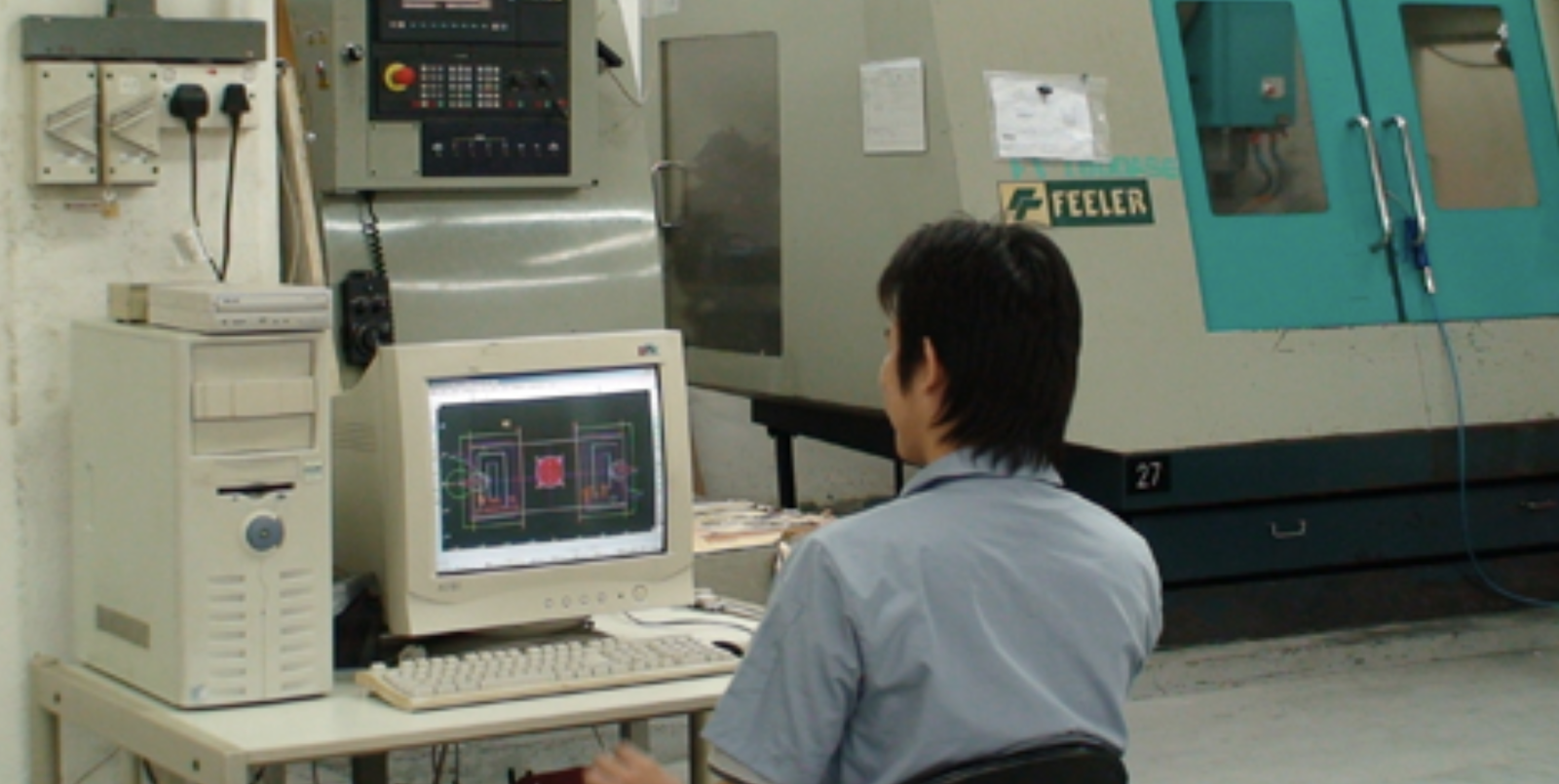
Image Credit: Slideshare - Junk computer, the tiny desk in the middle of the factory floor; yep, CAM
So, why can’t the original designer just do that instead? Good question. Neither CAD nor CAM are required to create a PCB. We can design a simple board using mylar and tape of varying thickness along with preformed geometries for the component footprints. The circuit was usually created at double the actual size and we would have a pair of targets that were, say eight inches apart but we would put down a dimension that indicated four inches. The mylar was reduced photographically to create the photo tools. Historically, all circuits were designed this way - until the advent of Gerber data.
Gerber technology used light-sensitive film and special aperture wheels in a machine that would shine a light through one of the peep-holes in the wheel. The diameter of the aperture would define the width of the line if it was a “draw” and the shape and size of the feature if it was a flash. During a draw, the correct aperture would be rotated in front of the light source and the film would be moved so that the light created lines on the board. Flashes would be done with the film stationary.
Someone had the job of setting up the correct aperture wheel that had 24 possible openings. There were common line widths and other shapes would be drawn by the creative use of the line apertures to fill in the geometry. This was a more direct approach that did away with reducing the enlarged circuits. When you’re eye-balling the air-gap every bit of breathing room helps.
Modern Times
From drilling to etching to finishing, the CAM documentation drives the boards through the shop. They figure out what you want and make it so.
Progress marches forward and the PCBs became so much more complex. So much so that it would be next to impossible to handle that much data manually. Welcome to the modern age. We now have CAD systems to generate a schematic that was previously drawn in pencil. An electronically generated schematic is more than simply a neater drawing with perfect text and straight lines. There are underlying data that get extracted by means of a net-list that drives connectivity at the board level.

Image Credit: Author - We can do our part by adding good labels
To begin with, schematic capture was done by the board designers but the Electrical Engineers eventually caught on as CAD became part of their curriculum. I’m not going to say that they like doing schematics as much as I did. Most don’t want to spend the time on a computer when there are better things to do in the lab. We, as designers, still serve as a backstop against any errors. A common one is when a wire is one pixel away from being connected to the pin. Of course, it is easy to misspell a net name during schematic capture. We feedback the corrections because we all want good products.
The CAM people do the same thing for the board designers. Their grandfathers swapped out aperture wheels because ours used 25 draws and flashes instead of 24. They figured out what grandpa wanted. Then they contrived to make a motley array of equipment produce that HiFi stereo everyone thought they wanted.
The modern CAM team keeps the gears turning when s*** gets real at 5 GHz and beyond. They want to fully understand the problem. Who do you think the fabricator turns to for a stack-up diagram? I’m slow. They can generate all that data in a snap. From drilling to etching to finishing, the CAM documentation drives the boards through the shop. They figure out what you want and make it so.
Planners shepherd the boards through the flow but it’s all based on the photo tools. Pre-distorting the data in what’s known as etch compensation means they micro edit the data globally. The process aim is to feed geometry into the line that ends with the product you imagined. The data you provide in whatever format will not be able to account for this type of thing.
Keeping up With Progress
It happens all the time. The PCB designer does everything that the internal team needs. The ultimate goal is to please everyone. If you can’t get that, then settle for everyone being equally “concerned”. Giving the fabricator’s liaison a chance to weigh in on material matters pays dividends down the road.
If your software is so-equipped you can make their job easier by running through the built-in manufacturability routines. The key to those programs is to start with reliable data. Vendor or standards-driven rules are going to be enforced anyway. So, yes, the CAD designer can do most of the work upfront. Although you can’t do everything, you may as well know what they are likely to say about your best effort.