Setting Up PCB Component Placement Tolerances
Key Takeaways
-
PCB component placement tolerances start with building correct footprints.
-
Electrical placement tolerances are essential for the board to run at its peak performance.
-
High-yield PCB manufacturing depends on how well PCB component placement tolerances are followed.
PCB component placement tolerances are critical for the best performance of the board
The word tolerance can mean a lot of different things depending on the context it is being used in. As a parent, my tolerance is something my children usually try to push to the breaking point. Similarly, in electronic design, tolerances are also usually pushed as far as they can go without breaking. The problem, of course, is what happens to the design when tolerances are exceeded.
When placing components on a printed circuit board, there are specific clearance tolerances that must be maintained. These tolerances include the specifications of the component footprint in the CAD system, how components are positioned for the best electrical performance, and how a part is placed for the manufacturability of the board. Let’s look closer at these PCB component placement tolerances and how you can set up your design tools to accommodate them.
PCB Component Tolerances
Before we look at the different tolerances of how components are placed on a circuit board, we need to first start with the part’s tolerances.
Each component footprint in the CAD system must be built according to its manufacturer’s specifications. If a CAD footprint is built incorrectly, the actual physical part may not fit on the metal land patterns of the circuit board. Problems like these can cause the board to not be manufacturable.
Building the component footprint within the PCB design system consists of two steps:
- Create the metal land patterns that the leads of the part will solder to. Land pattern dimensions can sometimes be found in the manufacturer’s datasheets or they may already exist as an industry-standard land pattern, such as a SOIC-14.
- Build the physical shape or outline of the component according to the specifications in the manufacturer’s datasheet.
Building PCB CAD footprints is a much more important part of PCB layout than most people realize, and it is important to understand why. Take a standard bypass capacitor in an 0603 package, for example. Depending on its density, your design may require hundreds of different bypass capacitors that come in the same 0603 package. You will only need one 0603 footprint in the design, and the CAD system will replicate it for each instance of a capacitor throughout the board. However, if it is incorrectly built, then all of those parts will be wrong. If the footprint is built too small, the actual parts may not even fit on the board, while a larger footprint may affect how the capacitors are soldered during manufacturing.
To avoid PCB component placement tolerance problems, keep these guidelines in mind while you are working with PCB footprints for your layout:
- Surface mount (SMT) land patterns need to be large enough to promote good solder fillets during PCB assembly. While these land patterns are usually specified in industry standards, there may be occasions when you have to create your own land patterns for special needs parts. In that case, make sure to build the land pattern to occupy both the minimum and maximum pin dimensions of the part.
- Thru-hole pads should be built with a drill hole large enough for component insertion yet small enough to prevent solder from wicking up through the hole.
- Component outlines should be constructed to the maximum material width specified in the manufacturer’s datasheet.
- Also, keep in mind that many land patterns will have to be used for the same part from different manufacturers. In that case, you will want to work with multiple data sheets to ensure that you allow for the maximum material widths for all parts.
At this point, your design should have good PCB footprints to work with, so let’s look at placement tolerances between parts for the best electrical performance of the board.
CAD footprints need to be built to precise specifications to ensure their fit and manufacturability
Placement Tolerances for Electrical Design Performance
When placing components in a PCB layout, one of the considerations to keep in mind is the component’s function in other parts. For instance, power supply components have strict placement requirements to ensure they produce as little noise and EMI as possible. These parts certainly must adhere to good design for manufacturability (DFM) requirements in their placement, but they also must be arranged for their best functionality. Here are some general placement rules to ensure maximum performance of your circuitry:
- Power supply components should be kept as close together as possible to minimize their trace lengths. Shorter and wider traces in power supplies lower the inductance and reduce electromagnetic interference (EMI).
- Bypass capacitors for large pin-count high-speed devices need to be placed as close as possible to the device’s power pins. This proximity will help to reduce current spikes and the resulting signal integrity problem of ground bounce.
- High-speed components connected through a signal path must be placed close together to prevent the signal path from wandering around on the board. A closely placed signal path will help ensure lower impedance in high-speed transmission lines.
- Keep components of functional partitions together except for where signals cross between the functional areas. This will prevent analog noise from contaminating digital circuitry and vice versa.
- For thermal management, keep hot-running components like processors and memory chips closer to the center of the board and separate power supply circuitry from each other.
These PCB component placement tolerance recommendations are designed to help your circuit board perform at its best. However, the circuit board still needs to be manufacturable, requiring a whole different set of placement tolerances.
PCB Component Placement Tolerances for Manufacturability
Even if your circuit board has the best made PCB footprints and precisely placed and routed components for performance, it’s all for not if the board can’t ultimately be manufactured. To ensure a board’s manufacturability, here are four key reasons why component placement tolerances must be obeyed.
Component to Component Spacing
Parts that are placed too close to each other can create potential problems for the following manufacturing processes:
- Automated assembly: The pick and place machines used to install components on the board will have difficulty with parts that are too close together, requiring those parts to be installed manually.
- Wave soldering: Small discrete parts need to be carefully placed for the direction that the board will travel through the wave. Two-pin parts should be placed so that both pins enter the wave simultaneously. Larger parts should not enter the wave before smaller parts to prevent shadowing, resulting in poor solder joints.
- Debug and rework: Smaller components should not be placed under larger ones to help assembly technicians debug and rework on the board.
Component to Board Edge Clearances
Care must also be taken when placing components close to the edge of the board for the following reasons:
-
Test: Parts close to the edge of the board can interfere with the vacuum drawdown of the test fixture.
-
Panels: Components that are too close to the board edge will require a breakout tab instead of V-grooves for depanelization. For boards with connectors, this is expected. Otherwise, the V-groove is a more cost-effective method of separating the board from the panel. Enough clearance also needs to be maintained to the board edge to prevent cracking of components or metal circuitry during depanelization.
-
Thermal: Parts near the board’s edges may interfere with the expected airflow necessary for cooling the board.
Test Point Clearances
Although not a physical component, test points need to be placed where the test fixture probes that come in contact with them will not collide with the parts on the board. The test points also need to have adequate spacing between each other for the test fixture probes.
Human Access
Most circuit boards have interface parts that have to be accessed by human hands. Switches have to be set, connectors will be plugged and unplugged, and certain nets will need to be probed with manual test equipment. Not only do these parts need to be placed where users can access them, but they also need to be placed with enough clearance to other parts that the user won’t risk collateral damage to the other parts in the process.
These DFM concerns can usually be worked around on prototype boards where quick-turn is critical to launching a new product. But when the circuit board enters regular production, these problems need to be corrected to help lower manufacturing time and costs. Thankfully, there are some features and utilities in PCB CAD systems that can help.
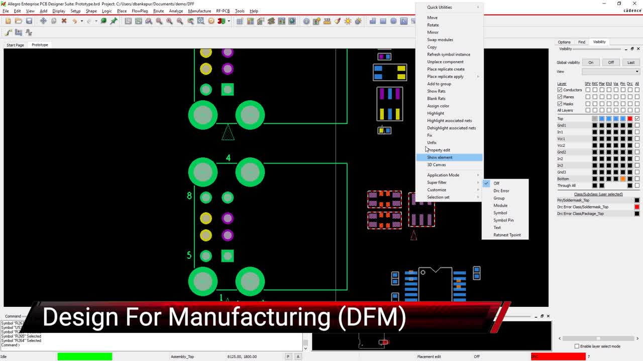
Using your CAD system’s DRC capabilities can save you a lot of grief, as shown here in Cadence Allegro
Using PCB Design Tools to Manage Component Placement Tolerances
The Unified Search utility, available in the Cadence Allegro design tools
As we have seen, using exact PCB footprints is essential for holding correct component placement tolerances. There are several aids to help with this, including industry standards and footprint creation wizards, but one of the best methods is to use exterior library services. Advanced PCB design systems usually have a utility that allows the designer to connect directly to an external library service to search for and download CAD models. In the picture above, you can see a picture of the Unified Search utility found in the Cadence suite of design tools. With the Unified Search tool, designers can find the parts they are looking for and download the manufacturer’s schematic symbol, SPICE models, datasheets, part information, images, and the PCB footprint. This utility will help ensure that the layout is getting the correct footprints to match the components used in the schematic.
There are other useful features in these design tools that can help as well. One of these is the constraint management system, which can be set up for different component clearances. Not only can you set up component to component clearances, but you can set up clearances for groups, areas, or even specific parts. Constraint systems like these will allow your design rule checking (DRCs) to alert you to component placement clearances that are not within tolerance and help you design a better circuit board.
To find out more about PCB layout and design for manufacturability, please take a look at this E-book.
If you’re looking to learn more about how Cadence has the solution for you, talk to us and our team of experts.