Considerations for Signal Plane Stackups
What You Can Learn:
-
Simple PCBs will generally work fine on a 2-layer board, but advanced designs need much more care to ensure signal integrity and power integrity.
-
For high-speed boards and high-speed/low-level boards, plane layers also need to be placed correctly to ensure power integrity and signal integrity.
-
Designing the correct layer stackup for your board also helps suppress crosstalk between signal nets and is required for controlled impedance in your PCB.
This dense board with high-speed components will need a multilayer PCB stackup.
Each layer in your PCB plays a specific role in determining electrical behavior. Your signal plane layers carry power and electrical signals between components, but they may not function properly unless you place the right arrangement of copper planes in the internal layers. Your PCB needs power and ground layers, in addition to signal layers, and you’ll need to place these in your PCB stackup to ensure your new board functions properly.
So where is the best place to put your power, ground, and signal layers? This is one of those long-debated questions in PCB design that forces designers to think carefully about their board’s intended application, how components function, and of the signaling tolerances in a board. If you understand the limits on impedance variations, jitter, voltage ripple vs. PDN impedance, and crosstalk suppression, you can determine the right arrangement of signal and plane layers to place in your board.
Turning your design intent into reality takes the right set of PCB design tools. Whether you need to create simple two-layer boards or high-speed PCBs with dozens of layers, your PCB design software needs to be adaptable for any application. Here are some important things to consider as you create your PCB stackup. With the PCB design features in Allegro, you can define your ideal layer stacks as templates for your boards, and you can design and analyze every aspect of your PCB.
How Many Layers Are Needed in Your PCB Stackup?
Introductory designers might tend to think in extremes when it comes to defining signal plane stackups. Either they only need two layers for every board or they need a dedicated layer for each small group of traces. The correct answer is somewhere in between, and it depends on the number of nets in your board, the acceptable level of ripple/jitter in your circuits, whether mixed signals are present, and much more.
In general, if your proof of concept will work fine on a breadboard, you can likely use any layout techniques you like on a two-layer board, and your board will most likely work properly. At most, you may need to take a gridded grounding approach for higher-speed signals (see below) to provide some minimum level of EMI suppression. For more complex devices that run at high speed or high frequency (or both), you’ll need at minimum a four-layer PCB stackup with a power plane, ground plane, and two signal layers.
The signal plane stackup on this board is only two layers, making it a bad choice for high-speed design.
The first consideration when determining the required number of signal plane layers should be the number of signal nets and the approximate width and spacing between signals. When you’re trying to estimate the number of signal layers you’ll need in your stackup, there are two basic steps you can take:
-
Determine net count: A simple net count in your schematic and your proposed board size can be used to get an estimate on the number of signal layers you’ll need in the board. Layer count is generally proportional to the fraction (net count*trace width)/(board width). In other words, more nets with wider traces require making the board larger or with more signal layers needing to be used. You have to default to your experience here to determine the exact number of signal layers you need to hold all your nets for a given board size.
-
Add in your plane layers: If you need controlled impedance routing for a signal layer, you now need to place a reference layer for each controlled impedance signal layer. If components are arranged densely, you’ll need a power plane below the component layer as you won’t have room for power rails on the surface layer. This can cause the number of required surface layers for high net count HDI boards to reach double digits, but the reference layers will provide shielding and consistent characteristic impedance.
Once you’ve determined the right number of layers for your multilayer board, you can move on to arranging your layers in your PCB stackup.
Designing Your PCB Layer Stack
The next step in your PCB stackup design is to arrange each layer to provide trace routing paths. Your layer stack is generally arranged symmetrically around the central core layer to prevent warping during high-temperature assembly and operation. The arrangement of plane and signal layers is critical for controlled impedance routing, as you’ll need to use specific equations for different trace arrangements to ensure controlled impedance.
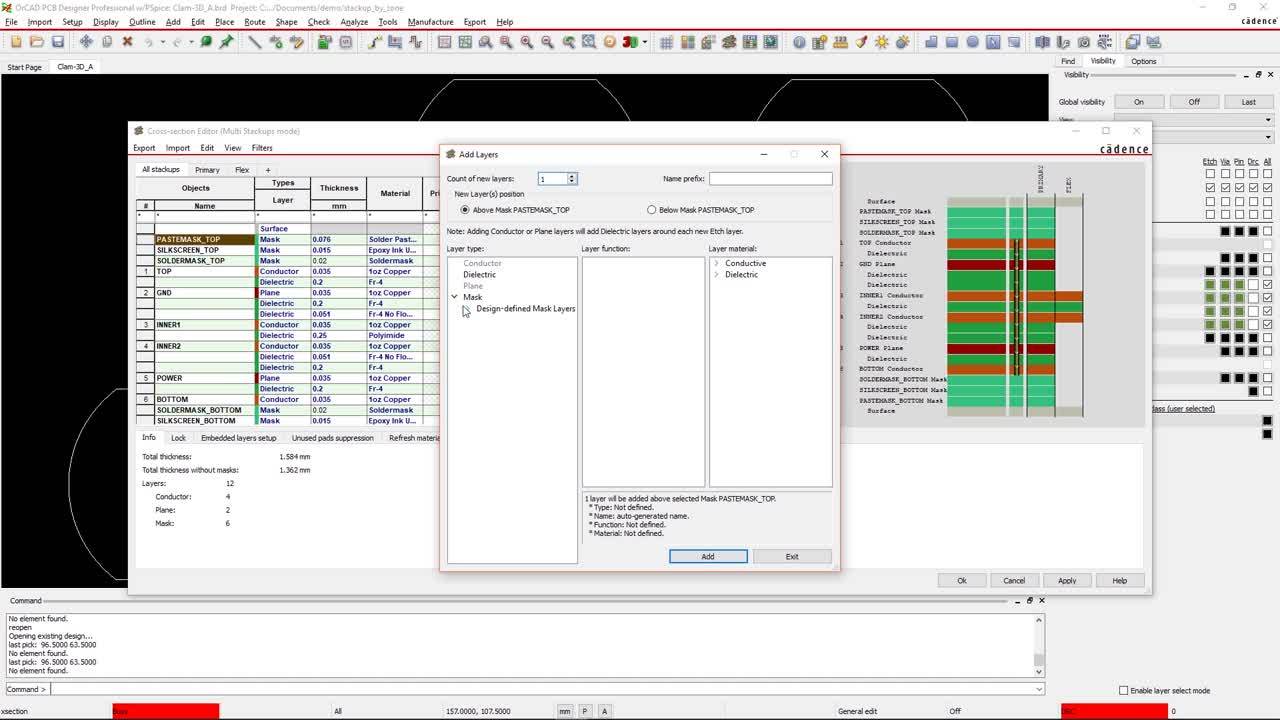
For rigid-flex stackup design, you’ll need to define different regions in the stackup for rigid and flex zones. The layer stack design tool in Allegro makes this process easy. After you capture your schematic as a blank PCB layout, you can define your layer stack and via transitions between different layers. You can then move on to determining the trace dimensions required for controlled impedance routing.
Stripline vs. Microstrip Traces and Controlled Impedance
For controlled impedance, your traces routed on internal layers between two plane layers should be designed using the stripline impedance equation. This equation defines the geometry needed for a stripline to have a particular characteristic impedance value. Because there are three different geometric parameters in the equation that determine impedance, it is easiest to determine the layer count you need first, as this will determine the layer thickness for a given board thickness. The copper weight for internal signal plane layers will usually be 0.5 or 1 oz./sq. ft. This leaves trace width as the last parameter to determine for a specific characteristic impedance.
The same procedure applies to microstrip traces on the surface layer. After determining the layer thickness and copper weight, you simply determine the trace width you need to use for a defined characteristic impedance. The PCB design tools in Allegro include an impedance calculator that will help you size your traces so that they have defined characteristic impedance. If you need to use differential pairs, you simply define traces in each layer as differential pairs and the impedance calculator will determine the correct spacing between traces.
Characteristic impedance calculator for a 4-layer board.
Checking Impedance in Your PCB Layout
As you route traces on a real board, they can couple to other traces and conductors capacitively or inductively. The parasitic capacitance and inductance created by nearby conductors alters the trace impedance in a real layout. To ensure you’ve met your impedance goals in all layers in your stackup, you need an impedance analysis tool that tracks impedance throughout select signal nets. If you can see unacceptably large variations that are flagged in your PCB layout, you can quickly select traces and adjust your routing to remove these impedance variations along an interconnect.
An example is shown below where large impedance variations along a trace are flagged in red. The separation between traces in this region should be adjusted to eliminate this impedance variation or to bring it within acceptable tolerances. You can define your required impedance tolerance in your design rules, and the post-layout impedance calculator tool will check your routing against your required impedance values.
Variations from characteristic impedance along two traces determined using the Impedance Workflow analyzer in Allegro.
Analog vs. Digital Sections and Your Layer Stackup
In the above discussion, we’ve only looked at digital signals, as they can be much more demanding than analog systems. What about fully analog boards or mixed-signal boards? For an analog board, power integrity is much easier, but signal integrity can be much more difficult. For mixed-signal boards, you need to combine the digital approaches shown above with the analog approaches presented here.
The bandwidth of a digital signal extends up to some high frequency, and the knee frequency is usually taken as the frequency for binary signals. The knee frequency is approximately 0.35/(rise time), which puts the knee frequency at 350 MHz for a signal with 1 ns rise time. For faster digital signals down to ~20 ps, the knee frequency now extends into 17.5 GHz. For analog signals, the bandwidth is much narrower, and you only need to worry about power plane impedance and insertion/return loss within this bandwidth. This makes power integrity and signal integrity much easier; any losses in the signal chain or high PDN impedance outside this bandwidth can be ignored.
An electromagnetic simulation model for an IC on a high layer count PCB.
Signal Isolation
The other option is more advanced and requires using grounded copper pour or via fences to ensure isolation between different sections of the board. If you run ground pour right next to the analog traces, you’ve just created a coplanar waveguide, which has high isolation and is a common choice for routing high-frequency analog signals. If you want to use via fences or other high-frequency conductive isolation structures, you should use an electromagnetic field solver to examine isolation and determine whether you should opt for separation in different signal layers instead.
Return Path Planning
Mixing analog and digital signals on a board places strict requirements on tracking the ground return path for displacement current and isolation between digital and analog board sections. Your board should be arranged so that analog return paths do not cross near digital components, and vice versa. This can be as simple as separating digital and analog signals into different layers separated by their respective ground planes. Although this increases costs, it ensures isolation between different sections.
If your analog components are drawing from an AC power source, your analog components may also need a dedicated analog power plane. This is a rare situation outside of power electronics, but it is conceptually easy to deal with as long as you can analyze return path planning. You can get away with dedicating a single power plane to both types of signals if you place the analog power section upstream and separated from the digital section. If you plan the return path properly, you’ll prevent interference between different power sections and ground sections. For DC power sections with switching regulators, switching noise from the DC section needs to be segregated from the AC section just like digital signals need to be segregated from analog signals.
Return path simulation in Allegro. This shows that the return path crosses over a gap in the ground plane (shown with the green arrow) creating a large loop inductance for this signal and making it susceptible to crosstalk.
Your stackup is a major determinant of signal and power integrity, and you need the right PCB design and analysis software to create a PCB around your desired stackup. The design tools in Allegro PCB Designer from Cadence integrate with a full suite of analysis tools for examining all aspects of signal and power integrity. This design platform integrates with powerful SI/PI Analysis Point Tools, giving you the analysis features you need to verify signal and power integrity in your next system. In addition, you can get more design tips in this E-book.
If you’re looking to learn more about how Cadence has the solution for you, talk to us and our team of experts.