High Density Interconnect Printed Circuit Boards: How to HDI
Memories: Looking back two years, the very first article I wrote for Cadence was titled “How to HDMI”. Due to popular demand, I’m dropping the “M” and diving into the pool of fine pitch layouts. The leading cause of HDI requirements come from the chip vendors. The original Ball Grid Array packages supported regular vias. Little by little, the pins got more cozy. 1.27 mm pitch became 1 mm then 0.8 down to 0.65 mm center to center. This was the final node where a plated through hole (PTH) vias was an option.
The next step down is 0.5 mm class BGAs. We can still use a through-via embedded within the solder pad but there are two issues. One is that the via has to be filled and capped so that you get a flat surface that doesn’t allow the solder to drain away during reflow. The other thing is that the typical “8/18” via has a finished hole size of 0.2 mm and a capture pad of .45 mm. On a 0.5 mm pitch device, that leaves 50 microns for a trace and an air gap on either side of the trace. That’s just not practical.
The Solution to Too Many Pins Per Square Inch: Micro-vias
A microvia is the first step into the HDI pool. The primary benefit is that micro-vias are er, micro! Besides their smaller size the real benefit is that micro-vias span one layer pair. You can “drill” from Layer 1 to Layer 2 and fan out on Layer 2 to a PTH via for the rest of the routing. That is the simplest implementation of HDI. It may be obvious to most of you but I’ll take a moment to point out that the “drilling” is done with a laser.

Image Credit: Author - The DSP side of a mixed signal PCB, note that ENIG finish is preferred to HASL of the first iteration above. The via-in-pad flatness improves with gold plating. On a side note, we transitioned to Cadence in the middle of this program to handle the HDI better. The gold one was my first Allegro board.
Actually, two lasers are better than one. There is a wavelength that cuts through copper and another that does a great job cutting into the dielectric material but mostly reflects off of the copper. You want to zap through the metal with an infrared CO2 Laser and then switch over to the ultra violet Neodymium-doped, Yttrium-Aluminum-Garnet (Nd-YAG) Laser to penetrate the insulation layer. Once it hits the inner Layer-2 metal, it stops pulsing without burning through the metal.
This is key. Even if you're going to stack micro-vias to go from Layer 1 to Layer 3, you still want the pad on Layer 2 as a target for the laser. There is a slight cost to stacking the micro-vias. I used the penny-pinching staggered-micro-via method on the Chromecast PCB. The drawback there is that it eats up a little more of the traditional Layer 2 ground plane. It took a few hours to implement the fabrication vendor’s request to do so. When you’re selling millions and millions of widgets, pennies matter. Note that in HDI boards, the ideal location for the ground plane isn’t necessarily Layer 2
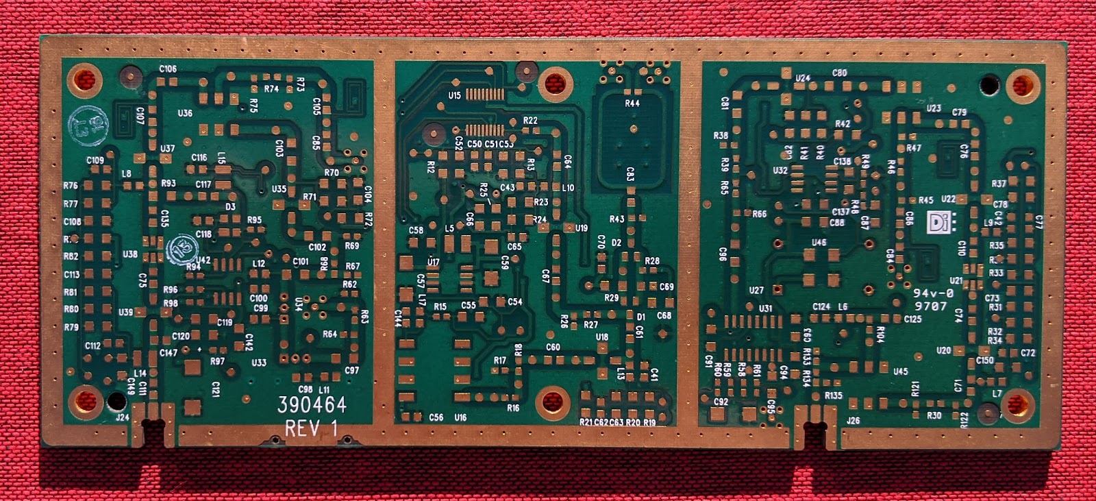
Image credit: Author - The thicker RF traces are required to allow test points without impedance issues. The traces can only be thick if the reference plane is a few layers deeper into the board.
So, there’s the size difference and the single-layer span but there is another factor to understand before you design a PCB with micro-vias. Once the hole is ablated of material, it has to be plated. It’s next to impossible to plate a deep and narrow hole so the dielectric material has to be very thin to use a micro-via. The ratio is somewhere between 0.6 to 1 and 1 to 1. Making the finished hole size the same as the dielectric thickness would be the leading edge and likely impossible for most fab-houses. You really want the material to be thinner than the hole diameter.
The Core of the Solution: Core Vias
What that means is that thin dielectrics are always in demand. Just as certain consumer products cost more these days, there may be some lead-time and price pressure on the HDI friendly materials. Balance between cost and performance comes with limited use of the micro-vias. I would say that a 3-N-3 stack-up is the sweet spot. Let me unpack the 3-N-3 thing. You start with a board that is N layers thick. For the purposes of discussion, we’ll call it N=4. The threes indicate the number of layers added around the core.
The shop will fabricate a 4-Layer board in the normal way using the PTH via geometry. That board will become the central core of the finished board. Then, they laminate one more layer on each side of the 4-Layer. Those layers are about 50 microns thick in order to support the 75-100 micron vias. They do that again and again, laminating and lasering so that you end up with three Laser-via layers, four mechanical-via layers and three more Laser-via layers for a total of 10 layers.
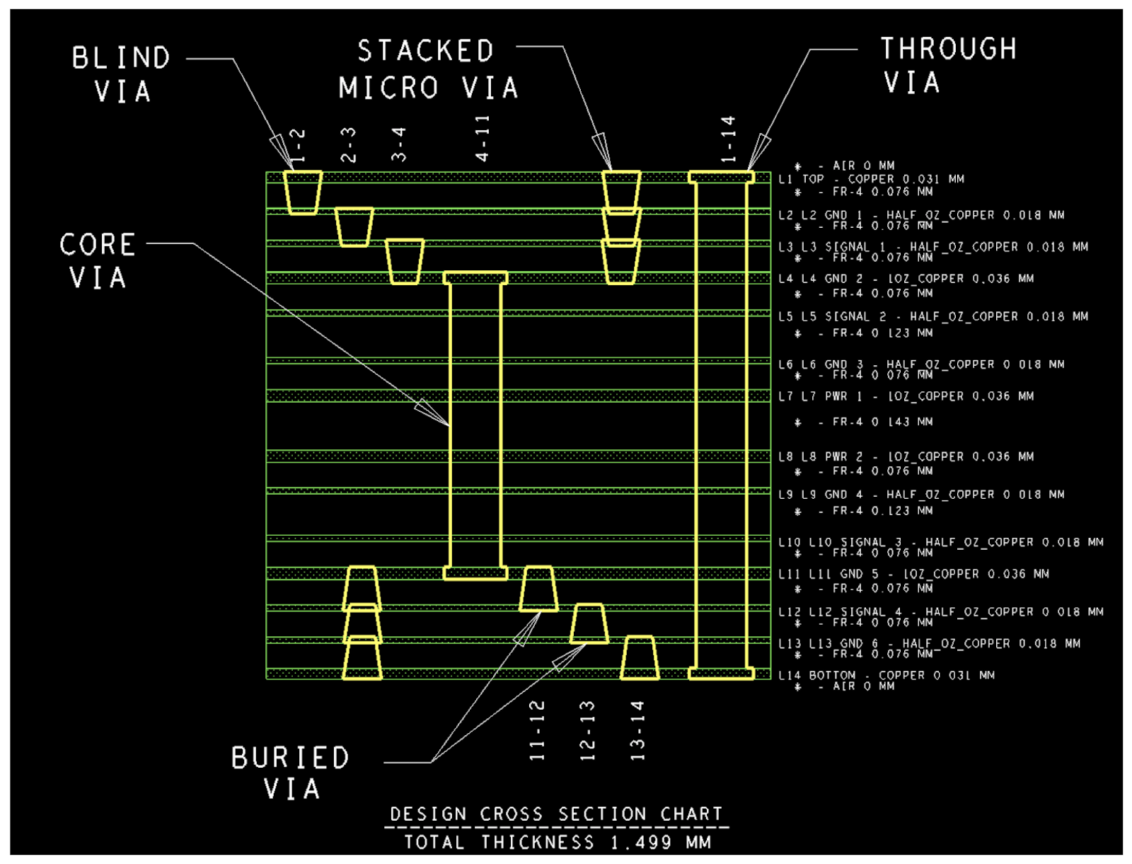
Image Credit: Author - A 14-Layer 3-N-3 stack-up; not necessarily to scale.
The main cost driver besides the thin prepreg layers is the lamination cycles. Starting with two, four, six or more core layers isn’t as big of a deal. That’s why the common terminology lumps all of those core stack-ups as “N” number of layers. It’s putting the board into the press again and waiting while it all gels together under the heat and pressure that drives cost. Presses are normally the most expensive pieces of equipment in the factory. They don’t work as fast as drills or plating tanks. A shop with one press has a bottle-neck and has to price HDI boards accordingly.
A Slightly Different Approach to HDI - My Favorite Stack-up
One cool hack is to fabricate the core of the HDI board using thin dielectrics on the outer layers and create microvias on the core before moving on the second lamination cycle. This is referred to as a 2-N-2 plus stack-up. It requires one fewer trips to the press than a 3-N-3 version. The penalty is that the core-via extends one layer further towards the top and bottom of the stack-up. The layers where the core-via protrudes are usually good layers for ground planes.
From a routing perspective having vias that span 1-2, 2-3, 3-4, 4-7, 7-8, 8-9, and 9-10 can solve most vexing fan-out issues. Many boards can be done with less technology and some may require micro-vias all the way through the board. By that point, the board is packed with components on both sides and probably has fine-pitch BGA devices with a thousand or more pins. When you finish one of those types of board, the feeling of accomplishment washes over you and your carpal tunnels like a tidal wave. Have fun with that.