OrCAD X: How to Manage Large PCB Component Libraries
Key Takeaways
-
Workspaces restrict team member view/edit privileges by file type to ensure library integrity on verified footprints.
-
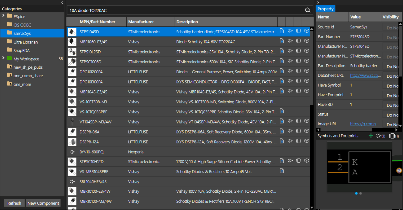
Component Explorer allows design teams to leverage footprint data on millions of components from leading vendors.
-
Librarians and designers will want to follow IPC-7251/7351 standards for naming conventions that make library search traversal a breeze.
Design teams wondering how to manage large PCB component libraries can look to OrCAD X and the Component Explorer.
Transitioning from the schematic to the layout requires accurate footprints representing the components' physical and electrical data. That’s why it’s crucial to verify footprints before netlisting designs, lest design teams see significant revisions late in product development that can severely strain timelines and budgets. Footprint validity becomes more pronounced when dealing with exceptionally large BOMs or vast master libraries containing thousands (or more!) of the footprints generated for an organization.
For designers and librarians wondering how to manage large PCB component libraries, OrCAD X features novel solutions that expedite workflow without sacrificing footprint accuracy or library integrity.
OrCAD X Tools for Component Library Management
|
Workspaces |
Allows team management and ensures data integrity through file-type view/edit privileges. |
|
Component Explorer |
Design teams can lean on verified footprints from leading component data vendors. |
|
Live BOM |
When component availability, lead time, or cost impede the current schematic, users can quickly locate replacement components and source datasheet information. |
Considerations for Library Management
Managing large PCB component libraries can be initially overwhelming due to the sheer number of components a project might have, not to mention the contents of the master library. Ultimately, the key to any library management is minimizing repeat work: components only need to be built and verified correctly once. After that, the footprint is valid, and librarians and designers can use it repeatedly without issue, provided no further changes occur to the footprint. Of course, changes to a known-good footprint are rarely malicious; instead, accidental changes introduced to the footprint design or duplication of work and use of unverified footprints are often the culprits.
While accidental, improper footprint library management can easily result in board scrappage when components no longer solder down, have incorrect pinouts, or have other manufacturing/netlist issues. OrCAD X gives design teams the tools to manage footprint access with the new Workspaces.
For small teams, Workspaces allows a team administrator to set file viewing and editing privileges for other team members - designers can edit design files but not library files, and vice versa for librarians. Admins can also designate a team member as a general user with only file viewing privileges. Ensuring that only the librarian or librarians have editing privileges for the footprint library is easier than ever to protect the integrity of correctly verified library entries.

Workspaces make it easy to manage file view/edit privileges among teams.
Building the library is another matter entirely. Components vary according to the packaging standard and pinouts according to IPC conventions. For example, it’s simple to create a simple chip component in a footprint wizard creation tool by plugging in the dimensions of the package and pad sizes (found in the manufacturer’s datasheet). It may be possible to adapt these “standard” footprints to match some irregular or otherwise unconventional components if the resemblance is close (i.e., similar package and pad dimensions, but perhaps a unique pinout, additional/missing pins, offset pin locations, etc.).
For some components, however, the package differs so significantly from conventional offerings that the most expeditious route for librarians is to create their footprints. In these cases, IPC-7251 and IPC-7351 offer standard practices for pad dimensioning (including through-hole sizing), courtyard spacing, and other critical footprint elements for a layout that adheres to manufacturing best practices while producing high yields and a low defect rate.
How to Manage Large PCB Component Libraries
Consistent footprint naming (covered under the IPC standards mentioned above) creates a unified, searchable library regardless of the building method for individual components:
-
Follow IPC naming conventions for footprints and pads to facilitate lookups and reduce the incidence of repeat items in the library whenever possible.
-
For footprints that don’t conform to the IPC naming convention, consider a straightforward naming scheme like the component MPN that captures both the component and any packaging variations. This system will differ between organizations, so discussing (or planning) with team members is best.
However, some organizations may wish to skip over footprint creation entirely for efficiency, team size, or time constraints. Fortunately, with OrCAD X and the Component Explorer, it’s simple to pair footprint data from trusted vendors to accelerate the design-planning phase and move to layout faster with verified footprints. Additionally, users can leverage schematic symbols and PSpice models through Component Explorer for a more expeditious schematic design and simulation stage.

Component Explorer allows design teams to leverage leading component footprint data vendors without ever having to leave the software.
Component Explorer and verified footprint data vendors can also be helpful when component procurement takes unexpected turns, like costly per-unit pricing due to supply crunches and long lead times. With Live BOM, users can stay ahead of the supply chain with up-to-the-moment component information on over a billion parts powered by Sourcengine. Live BOM makes finding equivalent, alternative, and drop-in replacement components simple for seamless and uninterrupted sourcing.

Live BOM makes finding replacement components simple with real-time market updates on cost, availability, and lead times.
Cadence Solutions for Library and Data Management
Smaller design teams wondering how to manage a large PCB component library can rely on OrCAD X features to expedite post-schematic planning and accelerate design timelines without sacrificing manufacturability in the layout. However, library management tools are not the only things the new platform offers: design teams can also benefit from collaborative cloud co-design and always-live manufacturing documentation that keeps the board and outputs in lockstep. Interested in learning more? See the complete Cadence PCB Design and Analysis Software list to see how you can take your PCB design to the next level.
Leading electronics providers rely on Cadence products to optimize power, space, and energy needs for a wide variety of market applications. To learn more about our innovative solutions, talk to our team of experts or subscribe to our YouTube channel.