Understanding the Electronic Manufacturing Flow
Key Takeaways
-
Learn the basics of electronic manufacturing flow.
-
Learn why PCB designers need to understand electronic manufacturing flow.
-
Explore methods to optimize PCBs for manufacturability.
Behind the scenes of a PCB manufacturing facility.
How do you make the perfect chocolate cake? I have no idea, but I’m pretty sure that sugar, eggs, chocolate, and flour are involved. However, I know that baking is a bit of an exact science, and it is not as simple as it may seem. Seeing as how I am not a baker, I let my indulgence of delicious chocolate cake be one of blissful ignorance.
However, it is risky to be ignorant of things directly in my line of work. As a PCB designer, it is valuable to have an understanding of the behind-the-scenes basics of electronic manufacturing workflow After all, it is still heavily connected to electronics design. Knowing what goes on in the manufacturing flow helps me to optimize my designs for better manufacturability. So, grab your forks and let’s dig in!
Electronic Manufacturing Flow: An Overview
The next time you get a chance to visit your PCB suppliers, try to get a tour around the facilities. You’ll be amazed at how the PCBs are made and assembled. If that’s not possible, here is an explanation of how designs are turned into products.
PCB Fabrication
The blueprint of your PCB, usually in Gerber format, is used to fabricate the PCB. PCBs are made of non-conductive substrates with copper layers. The circuit layout is transferred onto the copper layer using exposure methods, such as lithography
The supplier uses chemical processes to etch the copper layers according to the Gerber files provided. Solder masks and silkscreen are then applied onto the PCB. Tests, like flying probe tests, are then conducted to ensure the circuits are properly connected and there are no short circuits on the PCB.
Components Procurement
At the same time, you’ll need to start sourcing the components from suppliers. Usually, shipment takes at least two weeks depending on the number of components involved. There are a number of things that can affect supply chains (like global pandemics), so be sure to plan ahead if expediency is required.
PCB Assembly
Both the fabricated PCBs and components are then consigned to the PCB assembly supplier for mass production. Before starting the assembly, solder paste stencils are produced for the PCB. The process starts with applying solder paste to the pads of surface-mount device (SMD) footprints.
Then, the SMD components are fed into the pick-and-place machines where they are automatically placed onto the PCB. After all of the components are mounted, the PCB is placed into the reflow soldering machine.
After the SMD components are soldered, the assembler will manually solder any through-hole components.
Testing
All assembled PCBs must go through visual inspections. Often, X-ray machines are used to detect short circuits, discontinuity, or solder defects. Then, functionality tests need to be conducted on the PCBs before they are ready to be deployed.
Why Understanding Electronic Manufacturing Flow Is Important
While my chances of eating delicious chocolate cake are improved if I don’t try to make it myself, being oblivious to electronic manufacturing flow has gotten me into trouble. Once, I submitted a design with QFP footprints for production. Hundreds of those PCBs were then manufactured.
Understanding the process can help to reduce costly mistakes.
Imagine my horror when the PCBA supplier couldn’t accurately solder the QFP components, which are 100+ pins microcontrollers, because I missed out on the fiducial markers and tooling panel. I was faced with the choice of revising the design and fabricating a new batch of PCBs, resulting in overblown cost, or settling with a less-than-perfect assembly, which results in a higher reject rate.
Either way, I’ve lost money and time for failing to understand what goes on behind the scenes and how a designer could affect the process.
How to Optimize Your Design for Manufacturing?
It’s fair to say that PCB designers do have a substantial influence on the manufacturing process. Therefore, it’s important to keep manufacturability in mind when working on your design. Here are a few of the most important DFM considerations to remember:
-
ENsure the fiducial markers and tooling strips are in place.
-
Take note of the designators for the components and be sure they are placed near the footprints and are clearly visible.
-
Try not to put components near the edge of the PCB.
-
Keep SMT components on the same layer, as it reduces stencil cost and assembly time.
-
Communicate clearly at the start of the project. It helps if you understand the requirements and constraints of the manufacturer before designing the PCB.
-
Provide accurate Gerber files and inform the assembler of any important instructions.
Keep design for manufacturability considerations in mind.
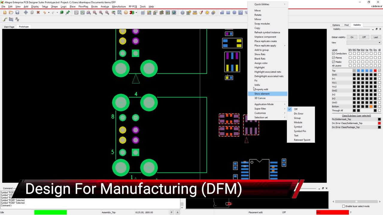
You’ll also want to consider using PCB design software that assists in creating better manufacturing-friendly designs. OrCAD PCB Designer allows for manufacturability rule checks that will ensure mistakes are spotted before committing the design for manufacturing. Having the right tools is the best thing you can give yourself with the aim of creating the best designs possible and avoiding costly mistakes or delays to market.
If you’re looking to learn more about how Cadence has the solution for you, talk to us and our team of experts.