Home
Free Trial
Home
Free Trial
Read More
Content
Filter
10 results found
Featured
Differential Pair Routing for Signal Integrity and EMI
Featured
Eye Diagram Analysis for High-Speed SI Validation
Featured
High-Speed HDI Stackups for Signal Integrity & EMI Control with Allegro X
Featured
Sneak Peek of Advanced Signal Analysis using OrCAD X Topology Explorer
Featured
Grounding and Return Paths: Power Plane No-Nos
Featured
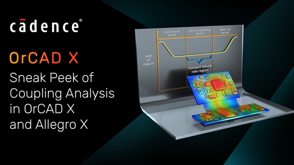
Sneak Peek of Coupling Analysis in OrCAD X and Allegro X
Featured
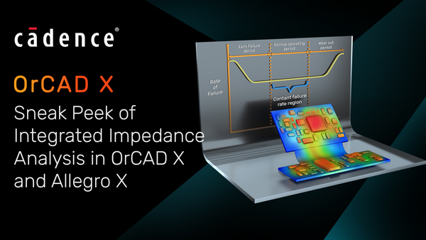
Sneak Peek of Integrated Impedance Analysis in OrCAD X and Allegro X
Featured
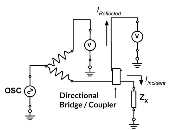
How Is Impedance Measured With Measurement Circuits?
Featured
Nyquist Sampling Theorem: Conserving Signal Characteristics
Featured
Ferrite Data Line Filters for Noise Suppression
Featured
Products
None
Allegro X PCB
(5)
OrCAD X
(2)
Sigrity X Aurora
(1)
Content types
None
Design Guide
(1)
Blog
(5)
Video
(4)
Solutions
None
Simulation & Analysis
(8)
PCB Layout
(4)
Schematic Capture
(1)