Circuit Net Labels and Schematic Organization
Key Takeaways
-
The problems with unorganized schematics.
-
Tips on making your schematic more readable.
-
How the right schematic capture tools can help.
The first step to a successful PCB layout is a good clean schematic.
It’s no secret among my family and friends that I like things in my life to be organized. My tools are sorted by category and size and hung on a pegboard in the garage. My important paperwork is filed in labeled folders in my desk drawer. Admittedly, this compulsive behavior does put me into the crosshairs of some sarcastic comments from time to time. But, when someone needs a specific tool or document, I can easily find it and suddenly I’m the hero again.
Another opportunity to be a hero is by creating a neat and orderly schematic that is easy to read and use. It goes without saying that a schematic sketched out on a napkin at lunchtime will probably be pretty disorganized. But, if your CAD schematics aren’t much better than a paper napkin, you are bound to have some big problems ahead of you working with your product. Let’s take a look at how to avoid some of these problems so that you can create a schematic that is more readable and easier to use.
Which Net Did You Say That Resistor Was Connected To?
There are a lot of ways that an unorganized and unreadable schematic can cause problems for your design:
-
Mistaken net names: Problems with circuit net labels are usually one of the first problems that you will see on a disorganized schematic. If the names are in the wrong locations or are unreadable, it can create a lot of confusion.
-
Missing components: If the parts aren’t laid out in an organized manner on the schematic it can cause some circuitry to be overlooked. A pullup resistor may be forgotten, or a power supply capacitor could end up missing if the circuitry is too spread out.
-
Incorrect connectivity: If components are not placed sequentially, it can be confusing to determine which net needs to be connected where. A memory bus may be connected backward, or other individual nets could get hooked up to an incorrect pin.
-
Incomplete information: Including the correct company contact information, logos, dates, sheet numbers, revisions, and copyright data is something that often gets forgotten on the final schematic. This can cause a lot of confusion for documentation tracking and may even result in legal problems as well.
-
Unstable CAD data: Ultimately, the schematic has to drive the layout in the CAD systems. An incorrect schematic will result in an incorrect layout, while a schematic with CAD errors in it may not even work with the layout tools.
-
Unusable for test and debug: If the schematic can’t be accurately read, it can’t be used. This will pose problems for test engineers, debug technicians, and eventually, field technicians too.
As you can tell, there are a lot of ways to mess up a perfectly good schematic. Next, let’s look at how to clean up these kinds of problems.
Creating a neat and organized schematic like this is not difficult with the right design tools.
Cleaning up Circuit Net Labels and Other Schematic Readability Problems
The first step in creating an organized and readable schematic is to figure out what you want the end product to look like. Obviously, you are going to be adding and deleting schematic sheets and circuitry as you go, but you can still start with a basic logic flow in mind. Using that as your foundation, figure out which pages will need to hold what circuitry and start building up the hierarchical organization for the schematic. Here is where using the different copy and repeat features of hierarchical schematic tools can be a big help.
The next step is to make sure that you are working from the drawing standards used by your company. If you don’t have any standards in place yet, now would be a good time to begin this practice. It is important to use text fonts and sizes that will be readable in the final schematic, as well as having all of your company contact and legal information ready to include. You want to make sure that you are using a grid size in your tools that will give your schematic the best readability and that all of your library links are in place for easy access.
A helpful tip here is to prepare a schematic template to work from so that you don’t have to recreate all the different settings each time you start a new schematic.
Finally, pay attention to all of the details in your schematic:
-
Make sure that your components are spread far enough apart to fit your nets and text but close enough so that the logic flow between parts is obvious.
-
Add the nets in a clean and organized manner, and avoid crossing nets over each other whenever possible.
-
Make sure to name your nets according to your company standards, and position your net labels where they can be clearly seen and read.
-
Fill in all of the required text to make your schematic a viable document: Design name, project name, part number(s), revision, date, company contact, logos, and copyright data.
It’s a good idea to keep these ideas in mind while you capture the schematic so that you don’t have to go back and do a lot of clean-up work later. Another good idea is to work with PCB design schematic capture tools that can help you create a good schematic instead of it fighting against you.
Property editors like this can make altering the attributes of a component easy.
Use the Full Capabilities of Your Design Tools
There are a lot of different capabilities within schematic capture tools that can help you create an organized schematic. Hierarchical tools can consolidate blocks of circuitry that have to be repeated without the need to draw each individual sheet. Library search tools can be used to get easy access to component manufacturer’s symbols, and part property edits, such as those shown above, are available for editing specific component information. There are also editing features to move components and nets around as well as drafting tools to help with the creation of title blocks or unique symbols.
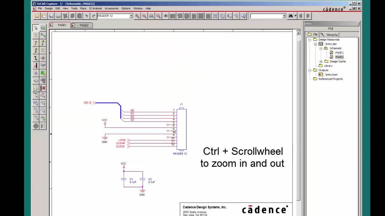
Thankfully, schematic capture tools like these are already available for engineers to use. One such PCB design system is from Cadence. OrCAD PCB Designer has all the features and functionality you need to create a great looking schematic each and every time. And with OrCAD, you not only have a great schematic capture tool, but you also have access to libraries, SPICE tools, and a host of other PCB layout tools.
If you’re looking to learn more about how Cadence has the solution for you, talk to us and our team of experts.