Tips on Transitioning from Schematic to Layout
Remodeling a room in your house is a common project that many homeowners take on. They will put a lot of time into visualizing what they want, picking colors and fittings as well as shopping for new furniture and appliances. But for all of that preparation, someone finally has to start construction in order for the dream to become a reality. Without swinging a hammer and sawing a couple of 2 x 4’s, all of that planning will have been for nothing.
In the world of PCB design, we have a similar process. A circuit board first starts out as a schematic to illustrate the circuitry using logic symbols and drawn net lines. Although the schematic does model the components and nets to create their connectivity, it isn’t the actual hardware design.
In the past, most electrical engineers would have created their schematic, and then sent it out for someone else to do the physical layout. Times have changed, however, and more and more engineers are stepping into the role of doing their own PCB layouts in addition to capturing the schematic. Part of the PCB layout process is now to transition the design data from schematic to layout. If this is the job that you find yourself facing, here are some tips on the data transferring process as well as some general PCB layout information to help.
The Differences Between Capturing Logic and Laying Out a PCB
If you’ve spent time working only with PCB schematics instead of circuit board layouts, you may not realize how truly different the two environments are from each other. The logic on a schematic is visual and must be created clearly so that it can be read and used by other people.
Although neatness does count when creating a schematic, it isn’t nearly as important as the neatness and precision in a PCB layout. If you have two symbols that overlap each other in a schematic, you will have a messy schematic. But two components overlapping in a layout will create a huge problem for manufacturing the board, and it probably will not be able to be built.
Another difference is that schematic symbols usually have to be placed on a grid in order to easily connect nets to their pins. On the layout side, however, those pins may end up being off grid depending on how the component footprint has been built. Some physical parts simply do not match a normal working grid in a CAD system, and the layout tools are designed to work with pins and connections that are off grid. Again, the key in layout is to maintain manufacturable clearances while the schematic needs to be tidy and on grid for readability.
Perhaps the biggest transition for a designer stepping into PCB layout is to start thinking in three dimensions. While having a 3D layout tool certainly helps in thinking three-dimensionally, I’m talking about the perception of the design; changing one’s view from simple symbol placement on a schematic sheet to an actual board with depth takes consideration. For instance, in a schematic, you will create high-speed logic for your design, but in the layout, you will physically design a high-speed board. This will include configuring your layer stackup to create a stripline structure to sandwich your high-speed transmission lines between two plane layers for the best signal integrity performance.
Now, with a 3D layout tool, especially one with capabilities like 2D and 3D cross probing, bend area visualization, and collision detection, you don’t have to let the 3D image reside solely in your imagination. With the Allegro 3D Canvas you can assuredly have your designs both checked properly and visually displayed for enclosure protection and mechanical teams working alongside you.
Editing the properties of a selected schematic part
Preparing to Transition Your Design from Schematic to Layout
In order to have a clean layout database to work with, you need to make sure that your schematic is clean and ready to go. Here are some steps that you should go through in order to make sure that you are ready to transition to layout:
-
A completed schematic: This doesn’t necessarily mean that the schematic won’t change during the design, ECO’s are a way of life after all. It does mean however that the schematic should be to the point where future alterations won’t completely change the intent of the layout.
-
Production parts: Make sure that you have updated all the temporary and developmental parts on the schematic before it goes to layout. If you aren’t able to do that, make sure to leave room to accommodate any PCB footprint changes that might still be on the way.
-
Duplicate circuitry: Check for and delete any unwanted circuitry that was created during copy and paste operations while the schematic was being captured. The last thing you want in layout is trying to fit parts on the board that doesn’t belong there in the first place.
-
Text: Make sure that all of the necessary company identification text, design notes, net names, and reference designators are in place and correct.
-
Design rule checks (DRCs): Even though your schematic doesn’t have to follow physical clearance rules as a layout does, it still needs to have its connectivity correctly captured. Most schematic capture tools offer DRCs to help you look for problems in the schematic, and below you can see an example of the schematic capture menu in Cadence Allegro. Make sure to run these checks and correct any problems in the schematic before you transfer the data to layout.
The DRC setup menu in Cadence Allegro
Working with Both Tools, the PCB Data Transition Process
Now that your schematic is complete and has passed its checks, it’s time to get that information into the layout database. Here are some of the tasks that you need to do in order to accomplish the layout to schematic conversion:
-
PCB footprints: For the netlist connectivity in the schematic to be successfully generated for the layout database, you will need PCB footprint data. If you have created your schematic using online component symbols, it is a good bet that the footprint data was already downloaded with the symbol. If your schematic has symbols from other sources however, you will want to check that those symbols are pointing to the correct footprints. You will also need to make sure that those footprint data files are available for the PCB database to access. If not you will either have to pull them into the design, or build them yourself.
-
Create the netlist: All of the different schematic tools have different mechanisms for doing this, but the process is essentially the same. After setting up the configurations for your specific schematic and layout databases, you will initiate the creation of a PCB netlist from the schematic. This netlist generally contains the following data for the layout database:
-
Components with reference designators and footprint names.
-
Pin information.
-
Net connectivity from pin to pin.
-
Component and net properties.
-
Design rules and high-speed constraints.
-
-
Create the PCB layout database: If one doesn’t already exist, you need to create a new layout database. This process will include the following tasks:
-
Create a board outline and layer stackup.
-
Pull in or build PCB footprints and other required design objects like vias.
-
Set up the parameters and additional design rules of the board.
-
-
Import the netlist: In the PCB layout database, you will now import the netlist that you have just created in the schematic. Again, different tools will have different mechanisms for doing this, but the ultimate goal of infusing the netlist connectivity into the layout database remains the same.
-
Check for errors: Even with all of the setups and schematic checks, there may still be some database problems that you didn’t expect. A classic example of this is a schematic symbol that doesn’t have the same number of pins that the physical footprint has. This is a common occurrence for unused pins on components, and it may not have any effect on the final operation of the board. But to avoid continual warnings popping up during the layout of the design, it’s best to correct it now.
Congratulations, at this point you should have successfully transferred your schematic connectivity data into your PCB layout. You are now ready to start placing parts in the layout and routing them.
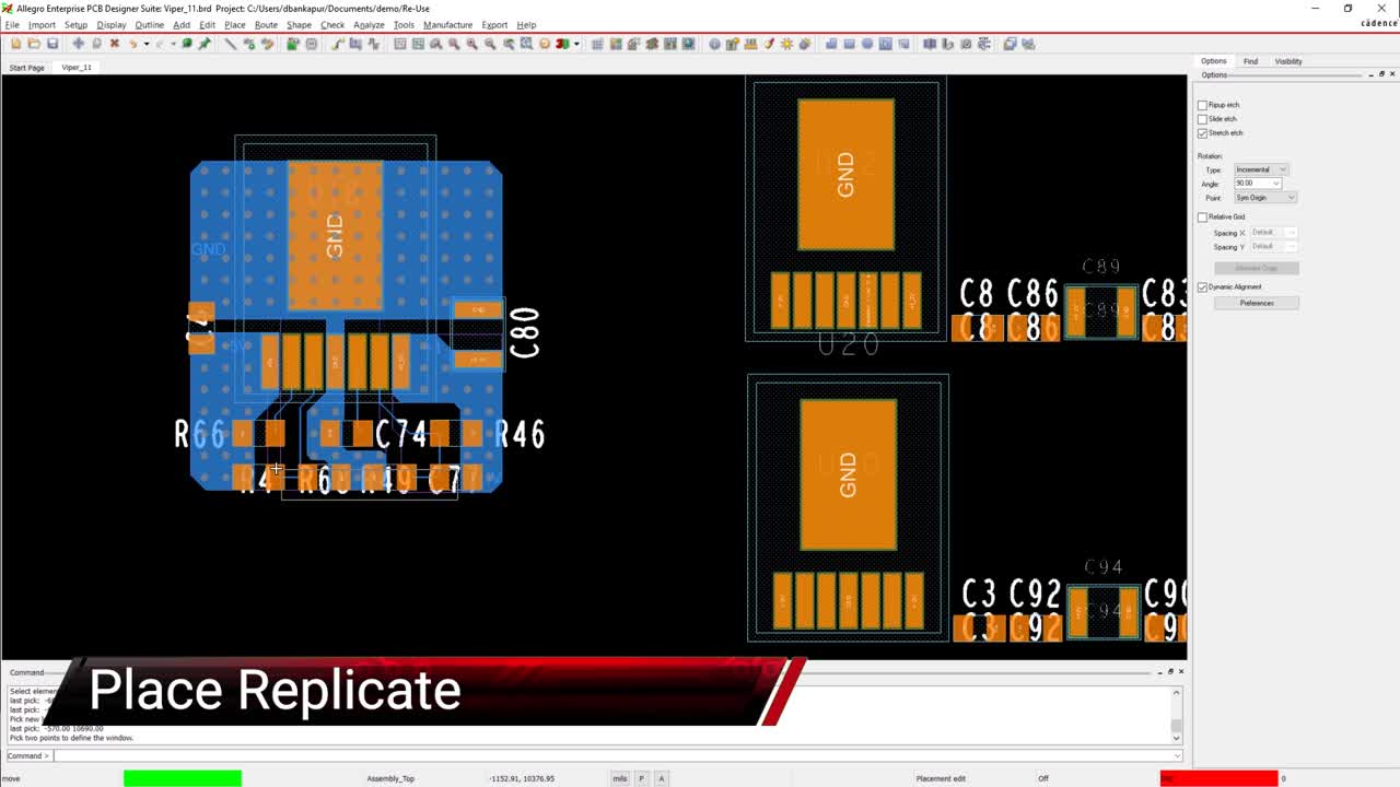
Components on a layout, placed and routed
For the Best Results, Use the Most Powerful Tools
PCB layout involves a great many steps, and synchronizing your schematic with the layout is just the first. In addition to place and route you will be managing the power distribution network of your board, and designing to rules set up to satisfy the requirements of PCB fabrication, assembly, and test. You will also be working with high-speed design constraints, and eventually transferring your layout data back to the schematic in order to update and annotate reference designators and other design information.
If you’re looking to learn more about how Cadence can assist in your design process, we have a host of online resources available for you to learn about important topics such as:
All of which start from these fundamentals: knowing how to build your schematic properly, and utilizing layout tools to the best of your capability.
To navigate these tasks successfully, you need the most advanced and powerful PCB design system available. Allegro PCB Designer from Cadence has all of the capabilities that we have talked about here and is ready for you to use on your next design. Not only will it provide you with the schematic and layout tools that you need, but Allegro will give you access to circuit simulation and power and signal integrity analysis tools, as well as a host of other features and functions.
If you’re looking to learn more about how Cadence has the solution for you, talk to us and our team of experts.