The Secret Language of the Printed Circuit Board Designer
The PCB Designer position is a hub where a lot of abstract and concrete information is funneled into a physical product. The boards start with the inspiration of an inventor. The idea is fleshed out in terms of the mechanical and the electrical requirements. Those two teams speak their own languages with just a little overlap.
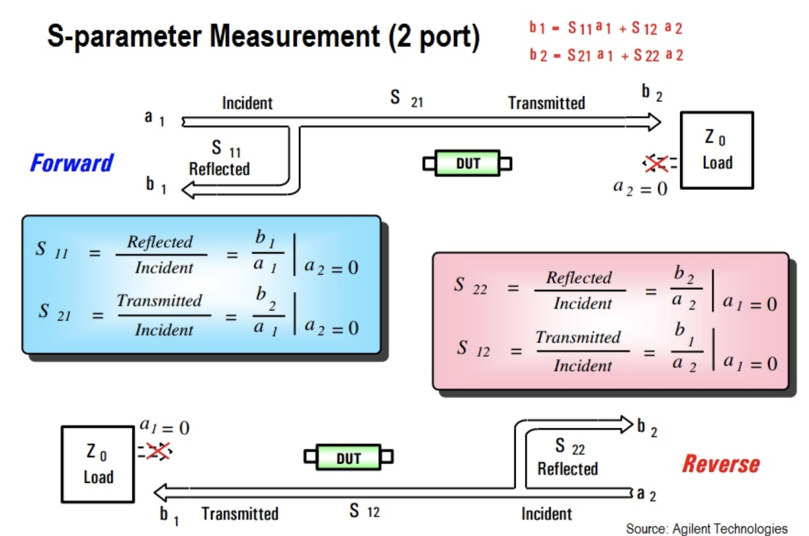
The signal integrity and power integrity experts add their own flavor. The signal integrity people “speak” primarily in S-parameters shown on charts that are “off the charts”. Their counterparts in the power integrity domain bring us tables of data augmented with power trees that trace the current from the main input to the last termination resistor. These people are a direct substitute for trial and error so we must accommodate their input as best we can.
The folks who plan and schedule our work will speak to us in Gantt charts, lead times, and Bill of Materials. Long tent poles and other euphemisms for bottlenecks are part of their vernacular. The time between the original component selection and the final artwork is enough for the procurement landscape to have changed. Show stoppers arise and an expediter gets involved. Remain calm and get them unstuck if there is anything you can do.
A reliability team is a normal part of research and development. The PCB and all of the parts are subject to scrutiny. The Component Engineers are fond of a number of phrases such as Mean Time Between Failure (MTBF) and use of the bathtub curve. Failure Analysis has them doing all sorts of destructive and non-destructive tests. Their methods are described in a sprawling document that may be familiar. IPC-T M-650 has many chapters; one is for cross-sectioning. They get a lot of data by slicing the board up after interrogating it from the outside.

Image credit: Lifewire
First Article Inspection is exactly that. The new product is subject to every dimensional or notational attribute on the drawing. Have a note or detail for everything that is required. Try to avoid asking for things that are not measurable. I can tell if a solder joint is well formed. I can’t look at it and be able to say if the PCB was baked prior to assembly. Processes are documented and maintained as separate documents.
This veers into syntax but is an important part of the way we communicate. We don’t want our drawings tethered to the process. Of course, your Manufacturing Engineer would like to include this stuff so that the operators on the assembly line only need one document in front of them. They mean well but they are wrong-headed on this matter.
If you accommodate this request, expect to get a negative comment from any auditors who may come along to certify your system. We live in a world where continuous improvement is the only option. Expect that you will be editing these drawings to keep up with the dynamic nature of production lines. It may be hard to say “no”. In the long run, it is the correct answer.
When I was teaching my fellow designers about military drafting requirements, one of the juniors came up to me after one lesson on geometric dimensioning and tolerancing and said that she liked the way I made words up such as “perpendicularity” and “parallelism”. Want to know how I knew that she had not read chapter 9 of the Mil-Std 100 Drawing Requirements Manual?
The DRM is a yellow pages size book that most drafters use as a reference. The link goes to the 84-page preamble loaded with definitions and other reference docs. Mil-Specs are always referencing other documents. One document calls out another that calls out others and in this way, the entirety of the Library of Congress seems to be in play when we discuss how to draw and label a picture.
Finally, we get to speak in the form of a data package that is ready to go. Gerber, Valor, IPC-2581 have all come along to replace the tape and mylar of the past. Each format comes in variations. We are creatures of habit and will make artwork in our comfort zone. I like easy. It is not easy when your fabrication shop has to ask for new or missing files. Stick to the one that works most of the time. There is a risk when you send two types of data. They say a man with two watches doesn’t know what time it is. You want your vendor to know.
Fabrication plants come with a host of processes and their own terms. Skiving? Desmearing? Delamination? Dendritic growth? What does it all mean? We better have some idea because we have to react to the technical questions from the CAM engineer. Those are usually sent to us at 8:45 PM on Friday. I’m not saying that they are buying time as the job is “on hold” until we agree to their stipulations, I’m just saying. You keep track when there are “ducks on the pond”.
Then, on to the assembly. It is rarely done in-house anymore because of the equipment costs and the potentially harmful byproducts. Still, we plunge into solder paste formulas, stencil thickness, pick-and-place data, careful silkscreen and assembly drawings all in an effort to keep the wheels turning. Solder defects come in many flavors. We’re expected to know about them and how to minimize their occurrence.
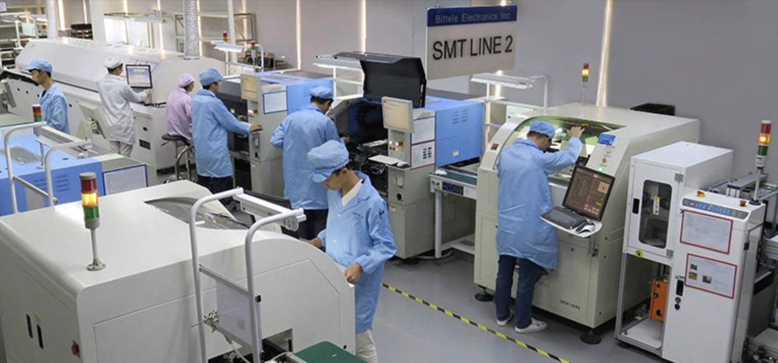
Image credit: 7PCB
The whole of that effort supports a series of transistor gates flipping bits on a massive scale for the software team. Yes, it is all ones and zeros but those digits are parsed in so many ways. Memory registers and that catalog the data are part of the so-called firmware. This is akin to the dimensions of the software. How many bits in a byte, whether there is a stop bit, or if you can transmit and receive at the same time - duplexing are some of the framework set up in firmware. Coders have their code and we’re better off for a little understanding.
As we work with the inventor, the EE, ME, SI/Pi, Buyer, Planner, Fabricator, Inspector, Tester, and other stakeholders, their lingo rubs off on the PCB designer. Signal Integrity software seems to favor inches while data sheets come mostly in Metric units. When we get below 4 mils (or 0.1 millimeters) we jump down to using microns. That is unless we measure gold, then it’s micro-inches. Of course, copper is measured in ounces and that’s another story.
“Deep sub-micron” has been replaced with nanometers for the technology nodes of our chips. We’re heading down to five nanometers so it may not be long before we’re talking picometers. Sub-atomic quantum computing is building things you can’t even see under a microscope. For all of these steps, we have adopted new words. Great words.