How to Add a Differential Pair in OrCAD X
Key Takeaways
-
Differential pairs require precise trace length matching and consistent spacing to maintain signal integrity and minimize skew.
-
OrCAD X simplifies differential pair creation with manual selection and auto-setup tools, allowing quick and accurate net pairing.
-
Applying Electrical Constraint Sets ensures compliance with impedance, spacing, and phase requirements for high-speed PCB designs.

Differential pair routing on a printed circuit board
A differential pair consists of two conductors carrying equal and opposite signals. These signals are referenced to each other rather than to a common ground, which enhances noise rejection, reduces crosstalk, and enhances signal strength.
In OrCAD X, designers can create and manage rules for differential pairs using the Constraint Manager. Once defined, specific design rules and constraints tailored for differential pairs, such as trace width, spacing, and phase control can be applied. This article will discuss how to add a differential pair rule within an OrCAD X schematic.
Key Differential Pair Parameters in OrCAD X Schematic Design
|
Parameter |
Description |
Typical Values |
| Trace Width |
Width of each conductor in the differential pair. |
6–10 mils |
| Pair Spacing (Gap) |
Distance between the two conductors in the pair. |
6–10 mils |
| Differential Impedance |
The combined impedance of the differential pair is crucial for signal integrity. |
90–110 Ω |
|
Length Matching |
Ensuring both traces are of equal length to maintain signal synchronization. |
±5 mils |
How to Add a Differential Pair Rule in an OrCAD X Schematic
Two primary methods exist to create differential pairs in OrCAD X: manual creation and automatic detection.
Manual Method: Creating Differential Pairs Manually
-
Select the Pair Nets: In OrCAD X Capture, identify and select both nets that will form the differential pair.
-
Right-Click and Create: Right-click on the selected nets, choose Create, and then select Differential Pair from the menu.
-
Name the Pair: Assign a unique name to the differential pair and click Create to finalize.
-
Alternative Method:
-
Navigate to the Object Menu, select Create, and click Differential Pair.
-
Alternatively, right-click on the Object Name, choose Create, and select Differential Pair to open the creation dialog.
-
From this dialog, manually select the two nets, assign a name, and confirm by clicking Create.
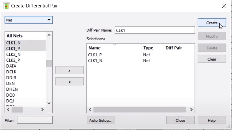
GUI within OrCAD X Constraint Manager for creating a differential pair. Shows two clock nets selected.
Automatic Method: Using Auto-Setup for Faster Creation
-
Open the Create Differential Pair GUI.
-
Identify a common suffix pattern for differential signals (e.g., _P and _N, + and -, _0 and _1).
-
Specify the suffix pattern in the Filter field (e.g., _P and _N).
-
Press Tab to automatically search the schematic for nets matching the pattern.
-
Click Create to generate differential pairs for all matching signals.
Once created, the differential pairs are visible in the Object List in the Constraint Manager.
Design Considerations for Differential Pairs
Differential signaling is standard in high-speed digital and RF applications, such as high-speed data buses (e.g., PCIe, USB, SATA), high-frequency RF signals (e.g., LVDS, Ethernet), and clock signals (e.g., DDR memory interfaces). The advantages of differential pairs include:
-
Reduced Noise Susceptibility: Any external noise affects both traces equally, and since the receiver only detects the difference, common-mode noise cancels out.
-
Lower Electromagnetic Interference (EMI): The equal and opposite currents in the pair generate opposing electromagnetic fields, reducing radiated emissions.
-
Higher Signal Integrity: Differential signals can maintain integrity over longer distances and across varying environments.
When routing differential pairs in a PCB layout, it’s essential to consider the following:
Factors that Impact Differential Pair Performance:
|
Design Guideline |
Importance |
Consideration |
| Matched Trace Lengths |
Prevents signal skew and maintains synchronization |
Length tolerance depends on signal speed; typically within a few mils |
| Consistent Trace Spacing (Coupling) |
Ensures stable impedance and signal integrity |
Uniform gap between traces; common differential impedances: 85Ω (USB), 100Ω (PCIe, Ethernet) |
| Minimized Via Usage |
Reduces impedance discontinuities |
Use fewer vias or back-drilled vias to minimize reflections |
|
Smooth Routing with Minimal Turns |
Maintains impedance consistency |
Use 45-degree bends or curved traces instead of sharp 90-degree turns |
|
Reference Plane Integrity |
Supports impedance control |
Maintain a continuous ground or power plane beneath differential pairs |
Defining Electrical Constraints for Differential Pairs
Differential pairs must follow specific electrical constraints to ensure proper high-speed signal routing. These constraints define spacing, width, and phase matching.
Creating an Electrical Constraint Set (EC Set) for Differential Pairs
-
Navigate to the Electrical Constraint Set Folder: Under Routing select Differential Pair.
-
Create a New EC Set:
-
Click on Objects in the menu, select Create, and then choose Electrical C Set.
-
Alternatively, right-click inside the folder and select Create → Electrical C Set.
Assign a Name: Provide a descriptive name for the new EC Set (e.g., Diff_Pair_Rules).
Configuring Differential Pair Constraints
-
Primary Gap – Defines the recommended spacing between the two traces of a differential pair without obstacles. Example: 6 mils.
-
Primary Width – Specifies the standard width of the differential pair traces. If undefined, the width uses the default PCB trace width setting. Example: 7 mils.
-
Neck Gap & Width – Important for routing in tight spaces (e.g., BGA areas). Typically set equal to the primary values with a small tolerance (e.g., 0.1 mils).
-
Minimum Line Space Check - This rule ensures that differential pair nets do not get too close. For example, if the default spacing is 8 mils, but differential pairs require 6 mils, this rule overrides the default.
-
Static Phase – Controls the allowable length difference between the two traces in a differential pair. Example: 200 mils.
-
Dynamic Phase Tolerance - This setting determines phase matching at bends. If left empty, OrCAD X uses the default values.
-
Uncoupled Length – Limits the length of an uncoupled differential pair trace. Example: 600 mils.
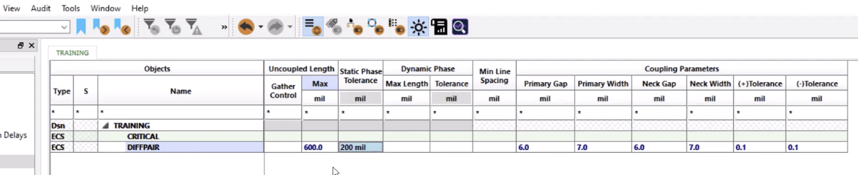
Configuring Differential Pair Constraints
Applying the EC Set to Differential Pairs
-
Go to the Net Folder: Select the Differential Pair category in the Constraint Manager.
-
Assign the EC Set: Locate the Referenced Electrical C Set column and apply the newly created EC Set to the differential pairs.
-
Verify Constraint Inheritance: All differential pairs will automatically inherit the defined constraints once assigned.
Setting differential pair rules in OrCAD X from the start ensures proper signal integrity and minimizes EMI in your PCB layouts. With Constraint Manager, automated pair detection, and robust electrical constraints, OrCAD X streamlines differential pair routing for optimal performance. Learn more about how to add a differential pair rule in OrCAD X schematic for your next design by trying it out with a free trial today!
Leading electronics providers rely on Cadence products to optimize power, space, and energy needs for a wide variety of market applications. To learn more about our innovative solutions, subscribe to our newsletter or our YouTube channel.