How to Create a PCB Library and Footprint Library in ORCAD X
Key Takeaways
-
Save unique footprints from a PCB design to reuse in future projects, reducing time and effort.
-
Shared libraries ensure standardized component usage, improving manufacturing reliability.
-
Create comprehensive libraries from projects for easy replication and collaborative design.
It’s easy to create a PCB library from an existing board file.
In PCB design, efficiency and consistency are key, and managing libraries effectively can significantly improve workflow. Two essential techniques in library management are creating a footprint library from a PCB and creating a PCB library from a project. These processes help designers streamline their work.
Imagine you’ve designed a complex PCB for a cutting-edge IoT device. The design includes custom footprints for rare or proprietary components. By creating a footprint library from a PCB design, you can:
-
Reuse Custom Footprints: You save these unique footprints for future projects, avoiding the need to recreate them for similar designs, such as a smaller or larger version of the IoT device.
-
Standardize Across Teams: Your team can ensure that everyone uses the same footprint for a particular component, maintaining consistency in manufacturing.
-
Streamline Outsourcing: When collaborating with external manufacturers or teams, you can share the exact footprints used, preventing discrepancies during production.
Create A Footprint Library from PCB
Creating a footprint library from a PCB involves extracting the physical layout designs (footprints) of all the components used in the printed circuit board (PCB) design and organizing them into a reusable library. Footprints are the physical representations of electronic components, and involve pads, outlines, and connection points, which define how these components will be placed and soldered onto the PCB. This process is particularly useful when you want to:
-
Reuse the same component layouts in future projects.
-
Share standardized footprints across different designs.
-
Maintain consistency and accuracy in component placement.
By generating a footprint library, you save time and effort in future PCB designs, ensuring that your work is both efficient and standardized.
OrCAD X PCB Editor users can define the export options.
Creating a Footprint Library from a PCB
|
Step |
Action |
Details |
|
1 |
Open the PCB Design |
Launch OrCAD X PCB Editor and load your existing PCB design file. |
|
2 |
Open Export Libraries |
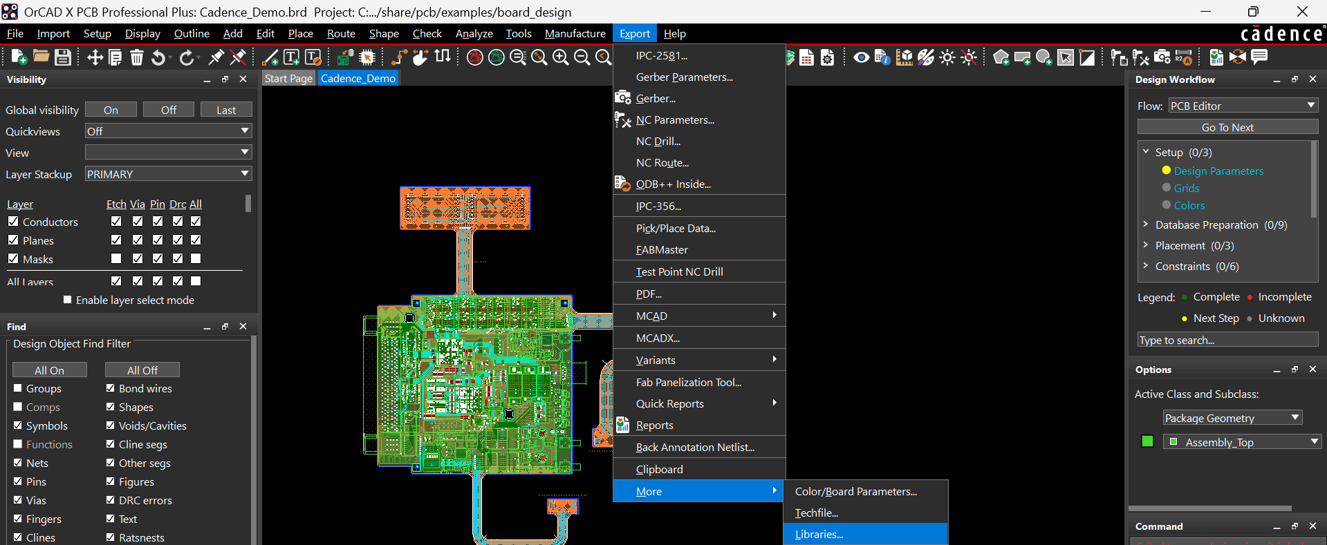
Navigate to Export > More > Libraries. |
|
3 |
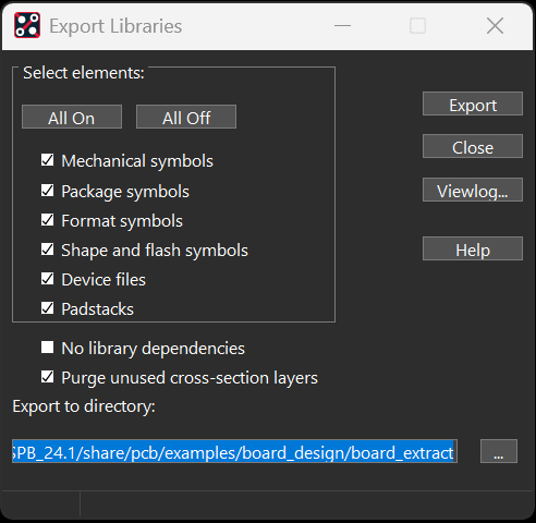
Extract Files |
In the Library Manager, select the file types you want to save and a destination directory.Use the Export function to save the package symbols, mechanical symbols, and padstacks. |
Create PCB Library from Project in OrCAD X
Creating a PCB library from a project involves compiling all the design elements of a PCB project, including footprints, symbols, and design rules, into a centralized library file. This library serves as a comprehensive reference for the components and configurations used in the project. It ensures that:
-
All customizations, such as specific component symbols and footprints, are preserved.
-
The design can be replicated or modified easily without starting from scratch.
-
The library can be shared with team members or used as a baseline for similar projects.
This process is particularly beneficial for teams working on collaborative PCB designs, as it enhances consistency and simplifies communication about the project's components and configurations.
Use Cases for Creating a PCB Library from a Project
When working on collaborative or large-scale projects, managing multiple components and configurations can be daunting. By creating a PCB library from a project you can:
-
Centralize Project Elements: All schematic symbols, footprints, and design rules are stored in one place, making them easy to reference for similar designs.
-
Simplify Collaboration: Teams working on different parts of the design can access the same library, ensuring consistency.
-
Create a Starting Template: If the project is part of a product line, the library serves as a foundation for designing variations of the product.
For instance, imagine a team designing a series of drones with similar features but different payloads. They create a PCB library from the initial project, including common components like motor drivers, sensors, and microcontrollers. For the next iteration, the team pulls components from this library, dramatically reducing the time spent sourcing and adding them individually.

OrCAD X Capture Users can quickly add a library to their PCB project.
Creating a PCB Library from a Project
|
Step |
Action |
Details |
|
1 |
Open the Project |
Launch OrCAD X Capture and open your project file. |
|
2 |
Create a New Library |
Go to File > New > Library. Provide a descriptive name for the new library. |
|
3 |
Add Components |
Within the new library, add components by creating new parts or importing existing ones. Ensure each component includes its schematic symbol and associated PCB footprint. |
|
4 |
Save the Library |
After adding all necessary components, save the library file in a location of your choice. |
Efficient library management is the cornerstone of streamlined PCB design, enabling designers to maintain consistency, reduce errors, and save valuable time. OrCAD X enables users to easily create a PCB library from a project, and create a footprint library from a PCB. Ready to take your PCB design process to the next level? Explore our PCB Design and Analysis Software to see how OrCAD X can empower your workflow!
Leading electronics providers rely on Cadence products to optimize power, space, and energy needs for a wide variety of market applications. To learn more about our innovative solutions, talk to our team of experts or subscribe to our YouTube channel.