Failed Schematic Capture Test? What A Designer Should Do Next
Key Takeaways:
- Define the purpose of schematic capture tests in your design workflow
- Learn how a schematic capture test can fail
- Understand the important takeaways from a failed schematic capture test
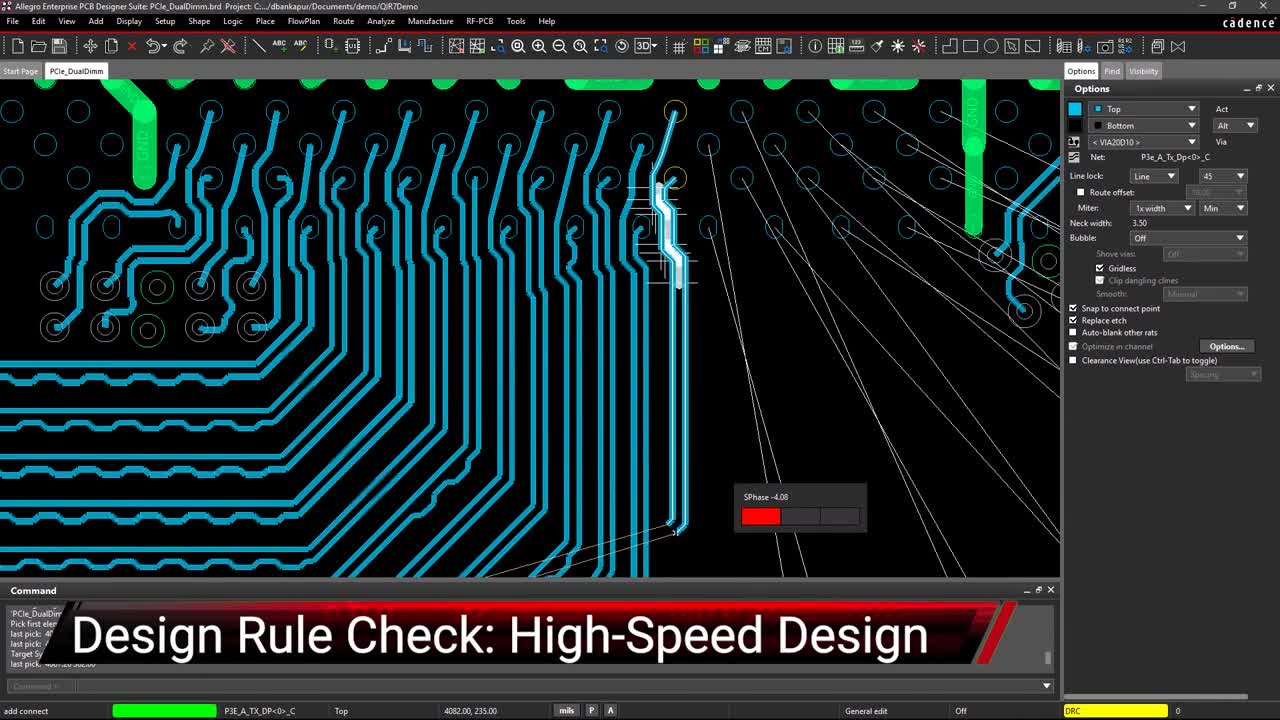
The schematic capture test ensures the design passes electrical check rules.
While entrepreneurs are harping on ‘making failure your best friend,’ it seems that my mom had a strong opinion. When I failed my history test in school, my mom went ballistic, throwing the wisdom-clad sayings down the drain. Left with no choice, I distanced myself from failure and started polishing up the historical facts.
In a way, I learned my lessons and aced every single history test since. Little did I know that failure and frustration wait at every single stage of a PCB designer’s career, and that this perseverance would come in handy in the long run. Thankfully, design software is now equipped with tools that detect and report failed schematic capture tests.
You’re about to learn what the schematic capture test is, and why it is important along with the repercussion for skipping this crucial point of your design.
What are Schematic Capture Tests
The process of a PCB design is roughly separated into two stages. The first involves creating the schematics on the software while the second stage is transferring the schematic into a layout format. In order to transfer the schematic information into the PCB layout, the software creates a netlist file, which contains symbolic information of the part and coordinates of the components.
The netlist is an important piece of information and must be error-free during the process. Therefore, PCB design software is built with a schematic capture test feature, which runs through the drawn schematic for anomalies and errors. The report will list the components or netlist involved and on the best software, you’re able to zoom in to the problematic location by clicking on the report items.
Common Types of Failed Schematic Schematic Capture Test
It’s common to assume that mistakes happen on the layout stage. While such an assumption is valid, equally devastating mistakes can occur when you’re working on the schematics. Here are some classic examples of what could go wrong during the schematic capture test.
1. Short Circuit
It is possible to mistakenly connect a power and ground pin in the schematic, or other nets that are not meant to be linked together. The schematic capture test ought to return an error when short circuits are detected.
Performing schematic capture tests pick up issues like a short circuit.
2. Disconnected Pins/Bus
Unless you specifically assign a component’s pin as ‘no connect’, the software will assume that it will be connected to another component. A more apparent violation of the rule is when a schematic connection line is left dangling.
Such violations usually triggered warnings during the test, but must be carefully inspected to ensure the circuit is functional and completely connected.
3. Duplicate Pins/Net Names
It’s easy for clumsiness to set in when you’re creating your own components. Duplicate pins, such as having a double pin 2 ought to be detected during the test.
Net names are usually automatically generated by the software, but there are times where designers alter the name for better identification. Mistakes can occur when the new net name overlaps with an existing one.
4. Flat/Hierarchical port connection
In complicated design, you’ll probably need to separate the circuit into different subcircuits. These subcircuits are usually arranged in either flat or hierarchical topology. In the former, all of the subcircuits share the same level while hierarchical designs are arranged in tiers.
Regardless of the arrangement, you’ll want to ensure that interconnecting ports of the subcircuits are linked. Otherwise, the schematic capture test may sound the alarm.
Why Responding To Failed Schematic Capture Tests Is Important
Getting a barrage of test failures can be annoying. Instead of turning the test criteria off, which you could in most software, you’ll want to inspect each of them. The repercussion of skipping a schematic capture test or ignoring the results is serious.
Schematic capture tests prevent unnecessary troubleshooting.
A short circuit, which goes undetected, could send your prototype up in smoke the moment it is powered on. Unconnected nets, which are brushed off casually, can result in hours of troubleshooting before locating the issue.
As a responsible designer, you ought to run through every single error or warnings and take the necessary steps. Fix the short circuit, join any unconnected nets and ensure the no duplicates of pins or net names.
Never take schematic capture tests for granted. You’ll want to have reliable PCB software working on getting the results right. With OrCAD PCB Designer you can rest easy with a schematic and layout tool that will ensure your board is secure throughout production.
If you’re looking to learn more about how Cadence has the solution for you, talk to us and our team of experts.