04 - Creating a Board Design
After the logic design is completed, the next step is to create the layout of the PCB. This section walks you through the basics of the layout creation steps, such as placement, routing, and generating output data to create a layout of the fan-control module design in the PCB Editor.
In this section, you will learn how to create a layout design tutorial.brd for the logic design you created and simulated in the previous sections. It includes the following tasks such as creating a board design and generating manufacturing files for the PCB and the flow of tasks required for creating a board design using PCB Editor:
For detail description of layout creation tasks, refer to the PCB Editor information set.
Creating a Blank Board
The first task is to create a new blank board design. Perform the following steps to create a blank board design:
- Open tutorial.opj in OrCAD X Capture.
- Choose PCB – New Layout.
Creating a blank board design in Capture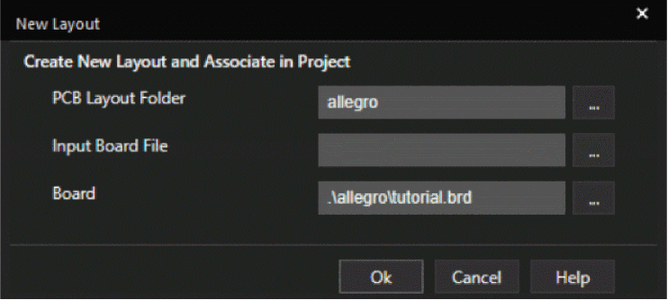
The new board design will be created in the default PCB Layout folder allegro inside the working project directory. - To create a blank board design, leave the Input Board File name field blank.
- Specify the output board file name as tutorial and click OK. The Cadence Product Choices dialog box is displayed.
- Select the OrCAD PCB Designer Professional w/PSpice option and click OK. A blank design tutorial.brd is opened in PCB Editor. The logic design data is transferred to the layout and is saved in the allegro directory.
Creating Design Outline
Design outline specifies the boundary within which components can be placed. It is necessary to create a design outline when transferring design data for ECAD-MCAD evaluation.
- In PCB Editor, choose Setup – Outline – Design.
The Active Class and Subclass fields are by default set to Board_Geometry and Design_Outline in the Options tab. - In the Design Outline dialog box, select Place rectangle and set Width and Height values to 2603 and 2333mils, respectively.
- Set Design edge clearance value to 10 mils. This value defines the space between the board outline and package and route keepin boundaries which is required to accommodate manufacturing tolerances, testing, and assembly.
A rectangular design outline is attached to the cursor.
Setting up design outline parameters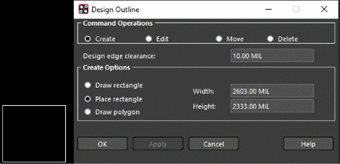
- Click anywhere in the design canvas to place the outline.
- Click OK to close the Design Outline dialog box.
A rectangular board outline is created with package and route keepin areas. - To view the entire board in the design canvas, choose View – Zoom Fit to center the board outline in the design window.
Design outline with package and route keepin areas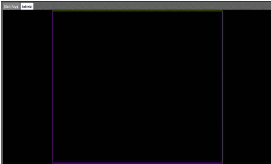
- Choose File – Save to save the design.
Placing Components
After creating the design outline you can start with component placement. All types of component symbols (discrete, ICs, mechanical, and format) can be placed either manually or by using automatic placement in the PCB Editor.
For this tutorial, place components interactively using the place manual command either in horizontal or vertical orientation using standard grid size of 25 mil, which makes them easy to align and assemble on the board.
- To start the placement, first enable the placement editing environment. Choose Setup – Application Mode – Placement Edit.
- Choose Place – Components Manually.
By default, Placement dialog box shows all the components listed by their reference designators. You can choose any reference designator and place it in the design canvas.
Selecting components from Placement dialog box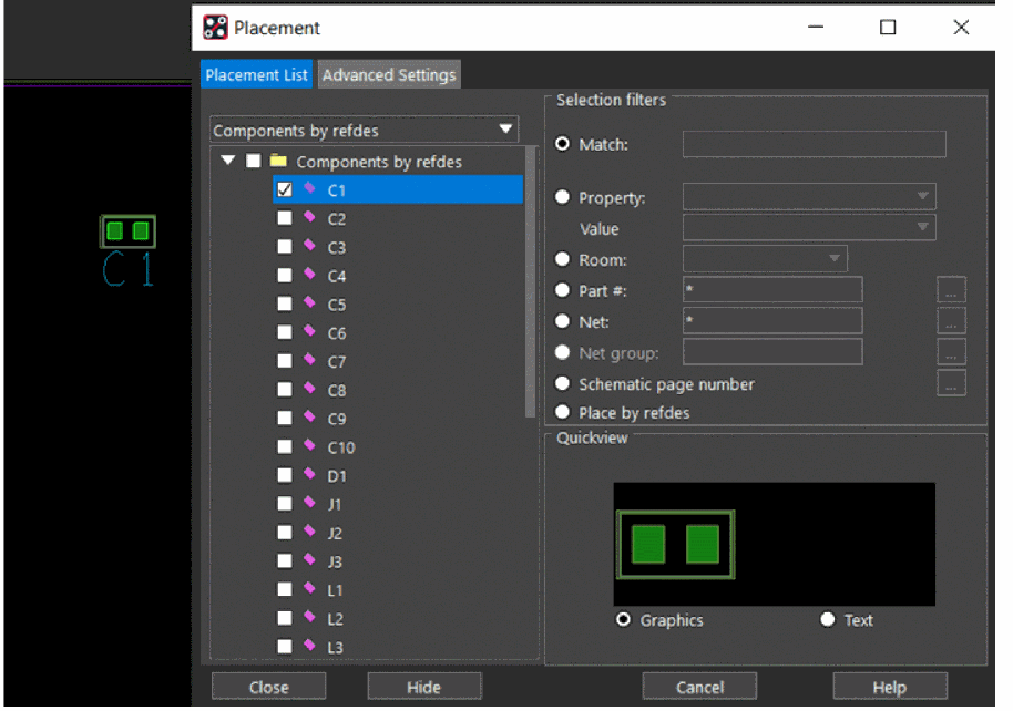
- Select the capacitor symbol C1.
The symbol gets attached to the cursor and is also visible in the Quickview window. - Right-click to choose Rotate. Use the handlebar to rotate the symbol by 90 degrees in anti-clockwise direction.
Rotating component before placing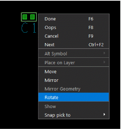
- Left-click in the design canvas to place the capacitor symbol.
- Similarly, select each reference designator one by one to place all the component symbols.
The following image depicts a sample placement.Place the symbols according to their logically connectivity. You can refer to schematic design to know which components are logically connected and must be placed closely.
Sample placement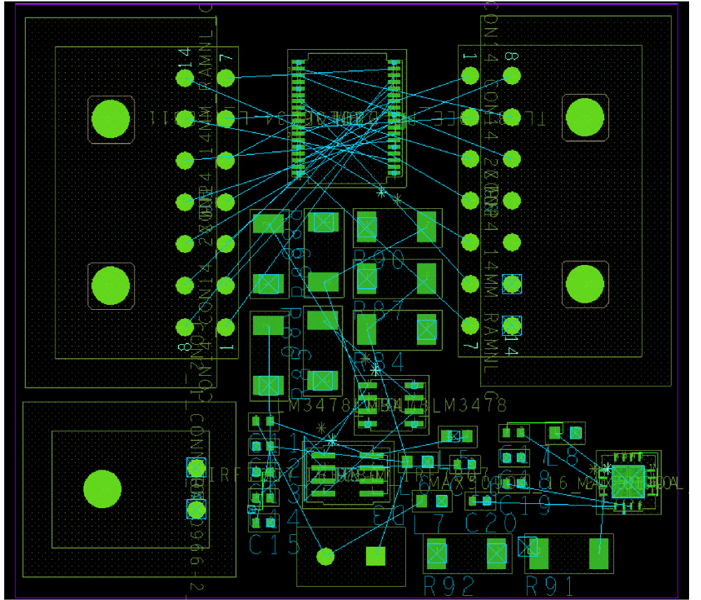
- Choose File – Save to save the design.
The placement is the most important step of the PCB design and impact all the subsequent steps of the layout design. If you choose to place components differently, the final routed board will also be different.
Setting Up Constraints
To meet manufacturing requirements you can configure the default constraint values in Constraint Manager either by creating constraint sets or by directly modifying the constraint values.
Before routing the board, specify the design constraints for routing. For this tutorial, specify two constraints for routing power nets: minimum thickness of the cline and maximum length of cline in neck mode.
- Choose Setup – Constraints – Constraint Manager. The Allegro Constraint Manager dialog box opens.
- In the Physical domain, choose Net – All Layers.
- In the All Layers worksheet, select the net 5V.
- Change the value of Min Line Width to 15 mil and Max Neck Length to 100 mil.
- Similarly, select the nets 3V3 and 0 and change the values for Min Line Width and Max Neck Length.
New values are displayed in blue color for the power nets. When routing, any violation to these values will create a DRC error.
Setting overrides for physical constraints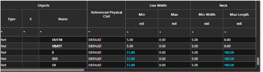
- Close Constraint Manager.
- Choose File – Save to save the design.
Routing Nets
Connecting the components in a layout is called routing. PCB Editor provides both manual and auto routing capabilities.
For this tutorial, use smart router for complete auto-routing.
- Choose Route – PCB Router – Route Automatic.
The Automatic Router dialog box opens and shows options to configure parameters for routing. For this tutorial, use the default values.
Automatic Router setup dialog box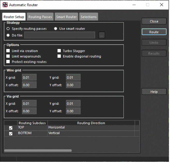
- To start auto-routing, click the Route button.
The auto-route process starts and takes a few seconds to complete. The auto-router considers the design outline and keepin areas while routing nets. - To verify that routing is completed successfully, choose Display – Status.
Status dialog box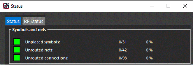
The Status dialog box confirms that all the nets are routed. - Click OK to close the Status dialog box.
- Close the Automatic Router dialog box.
The following image shows a routed board design.
Auto-routed board design sample
- Choose File – Save to save the design.
Renaming Components
After you have completed the placement and routing you can reorder the reference designators of components on the board in a specific pattern. This steps makes the testing and assembly process easier.
- Choose Logic – Auto Rename Refdes – Rename.
The Rename Refdes dialog box opens showing grid settings and option to select all the components for renaming action.
Rename Reference Designators options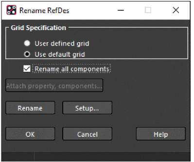
- Click the Setup button to specify more options.
The Rename Ref Des Set Up dialog box opens. - In the Reference Designator Format section:
Remove layer identifier for TOP and BOTTOM layers.
Enable the Preserve Current prefixes check box.
Rename Reference Designator Set Up dialog box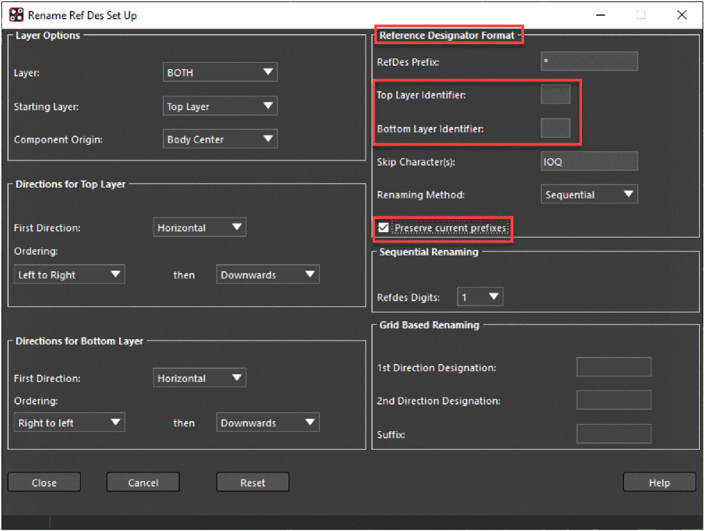
- Close the Rename Ref Des Set Up dialog box.
- Click the Rename button in the Rename RefDes dialog box.
Renaming of reference designators starts from the upper-left corner of the board in the horizontal direction and the numbers are increasing in the downward direction.
Board design with renamed reference designators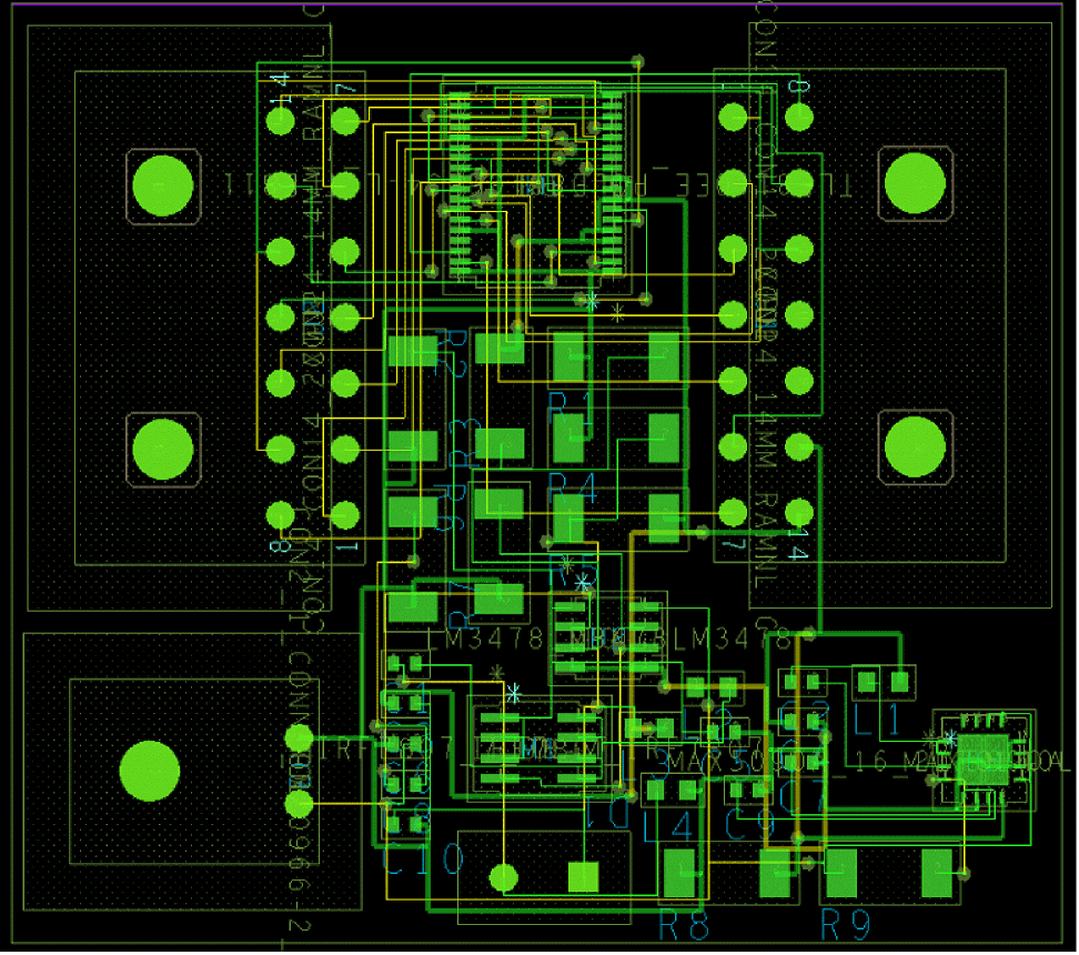
- Click OK to close the Rename RefDes dialog box.
- Choose File – Save to save the design.
Visualizing Design in 3D
The built-in 3D visualization tool of PCB Editor lets you preview the board design at any time during the design. You can open the design in 3D Canvas and verify the design as a complete assembly.
To analyze the design in the 3D Canvas, 3D models must be assigned to all the symbols. You can map a 3D model either at a symbol level or at the design level. PCB Editor, by default, supports STEP models for 3D visualization. For the components used in this tutorial, 3D models are assigned at the symbol level.
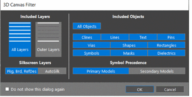
- Choose View – 3D Canvas. A 3D Canvas Filter dialog box opens. Click OK to proceed.
 A progress bar displays while loading the design into 3D Canvas.
3D view of board design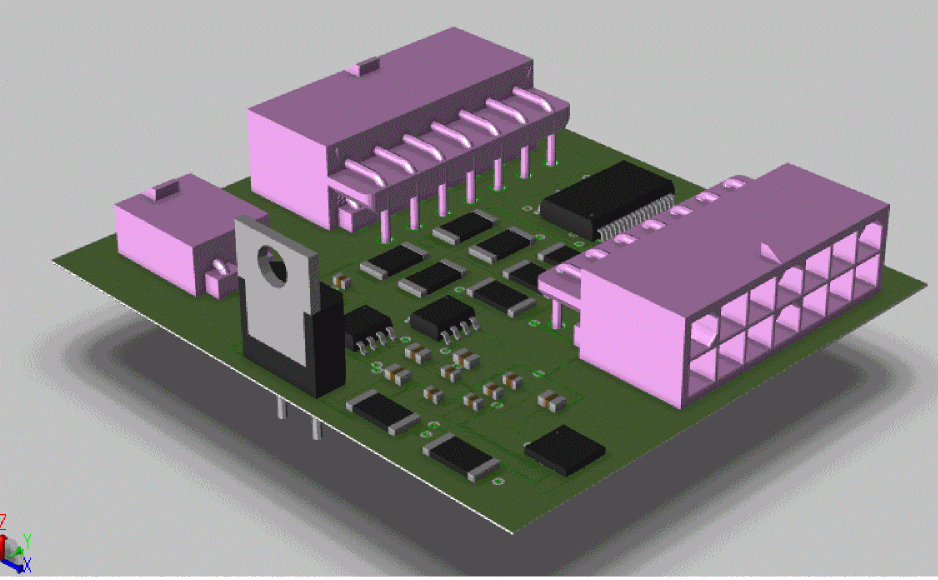
- Choose View – Camera options to view the design in different perspectives.
- Close 3D Canvas.
Generating Manufacturing Files
The final task is to generate various types of output files of the physical design data. You can create Gerber files, Excellon NC Drill files, DXF files, IPC2581, ODB++, and printer/plotter files.These files are standard files and are required by the fabrication houses to manufacture a PCB.
For this tutorial, create three types of output files:
- Artwork (Gerber)
- NC Drill
- IPC2581
Creating Artwork
To create artwork files, PCB Editor reads film control records to determine the number of artwork files to produce, their names, and list of classes and subclasses to include in each artwork file.
To specify classes and subclasses for an artwork file, use Color Dialog to set the visibility of required classes and subclasses.
- Choose Display – Color/Visibility.
The Color Dialog opens.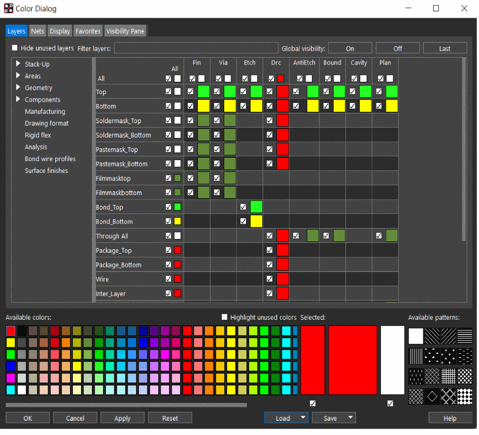
- In the Layers tab, click the Off button for Global Visibility.
The visibility of all the classes and subclass are turned off. - Expand the Stack-Up – Conductor folder, select Soldermask_TopandPastemask_Toplayers and enable the check box for Pin only.
The soldermask and pastemask layers of pins becomes visible in the design canvas. - Similarly, in the Geometry folder, select Soldermask_Top andPastemask_Toplayers and enable the check box for All objects.
The visibility of soldermask and pastemask layer is set on both board and package geometry. - Click OK to close the Color Dialog.
- Choose Manufacture – Artwork.
The Artwork Control Form opens which reads the cross-section and auto-generates one film record for each etch subclass and includes etch, pins, and vias.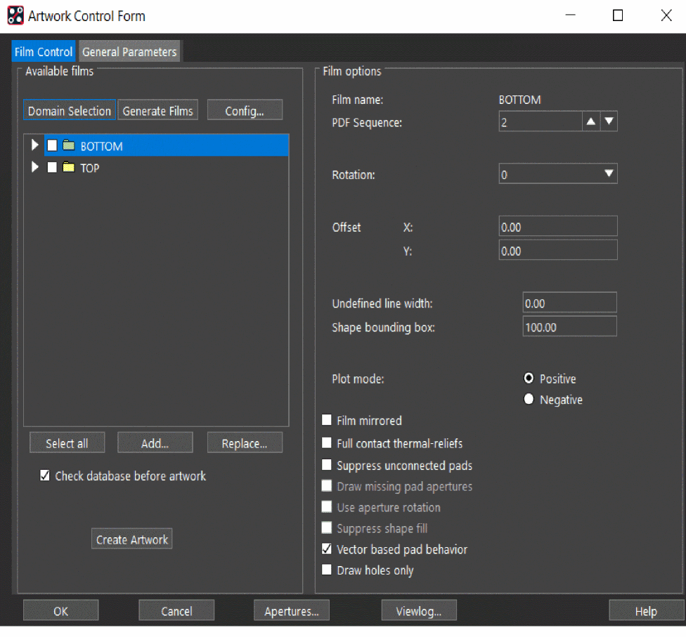
- In Artwork Control Form, select both the TOP and BOTTOM layers.
- Click Create Artwork to generate artwork.
Artwork generation settings
Two artwork files (TOP.art and BOTTOM.art) are created in the allegro directory. - Click Viewlog to review the log file.
- Click OK to close the Artwork Control Form.
Creating NC Drill
NC Drill output files are created for numerically-controlled (NC) drills and router and helps in assessing the cost of PCB manufacturing. The drill output files include drill legend tables and drill files.
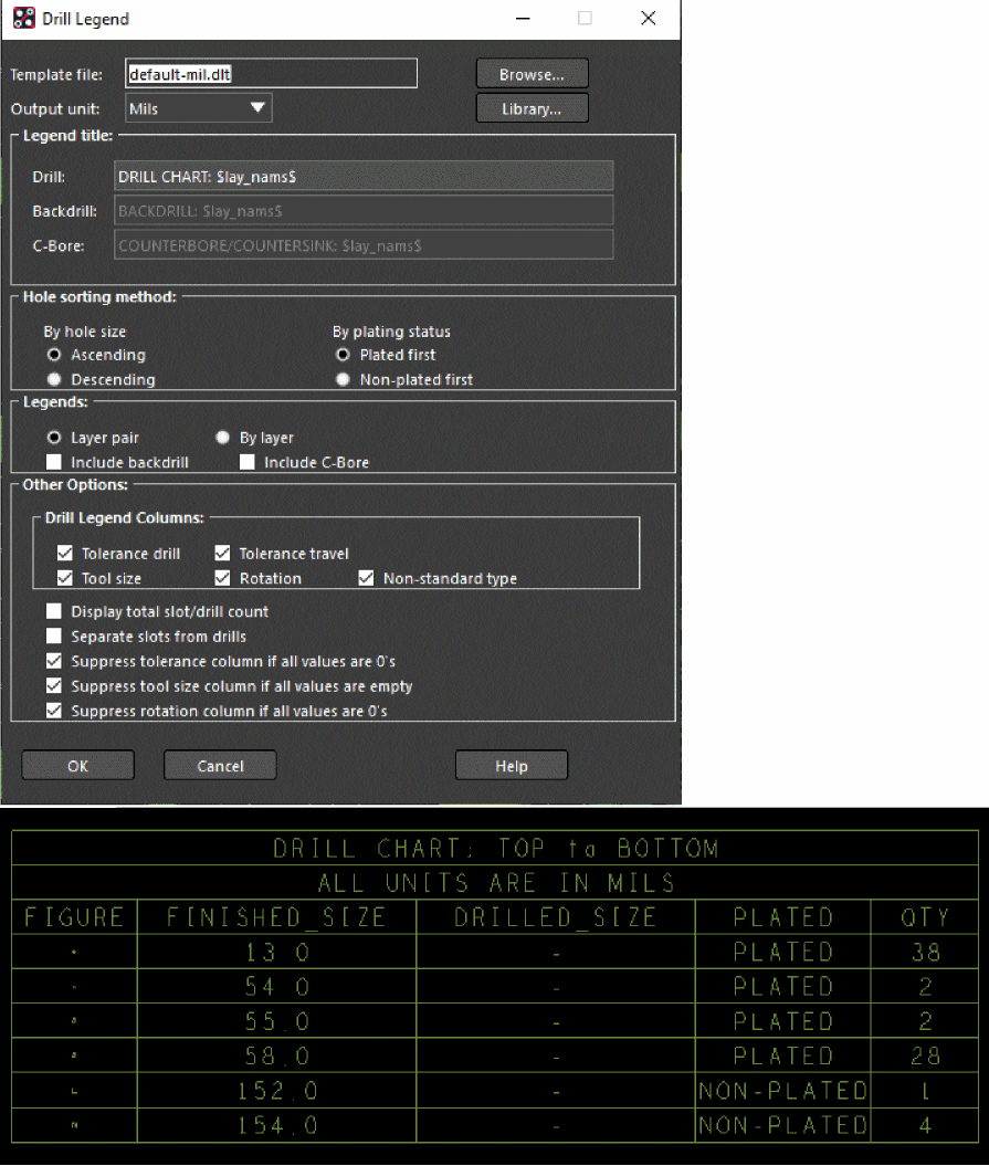
Generating Drill Legend
Drill legend tables are used in fabrication drawing and show the number, type, and tolerance of plated and non-plated holes in the design.
- Choose Display – Color/Visibility, click On to enable Global Visibility and click OK to close the dialog box.
- Choose Manufacture – NC – Drill Legend.
The Drill Legend dialog box opens. - Click OK to generate the drill legend symbol.
The drill legend symbol gets attached to the cursor. - Left-click to place the drill legend in the design canvas.
Drill Legend parameters and table
Generating NC Drill
The NC drill file is created based on the parameters specified for the drill coordinate data format.
- Choose Manufacture – NC – NC Drill.
The NC Drill dialog box opens. - Click Parameters to open NC Parameters dialog box.
- Enable the Enhanced Excellon format check box.
A header in the NC Drill and NC Route output files is generated that uses Excellon commands. - Click OK to save the parameters.
- Click Drill to generate the drill file.
NC Drill setup options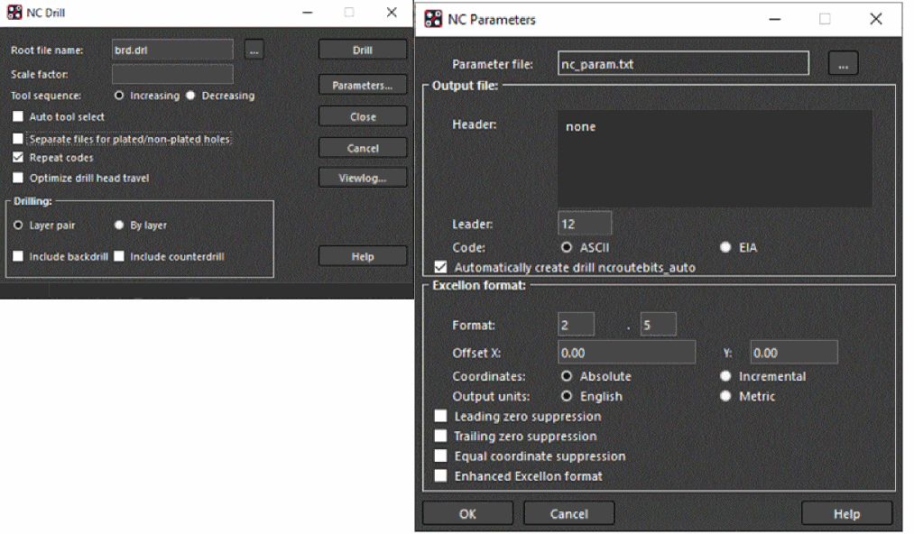
The NC Drill file (tutorial.drl) is created in the allegro directory. - Click Viewlog to review the log file.
- Close the dialog box.
Creating IPC2581 Files
IPC2581 is an XML-based data exchange format used for providing physical design data for fabrication and assembly of PCBs.
For this tutorial, create IPC2581 output using default values.
- Choose File – Export – IPC2581.
The IPC2581 Export opens.
Generating IPC2581 output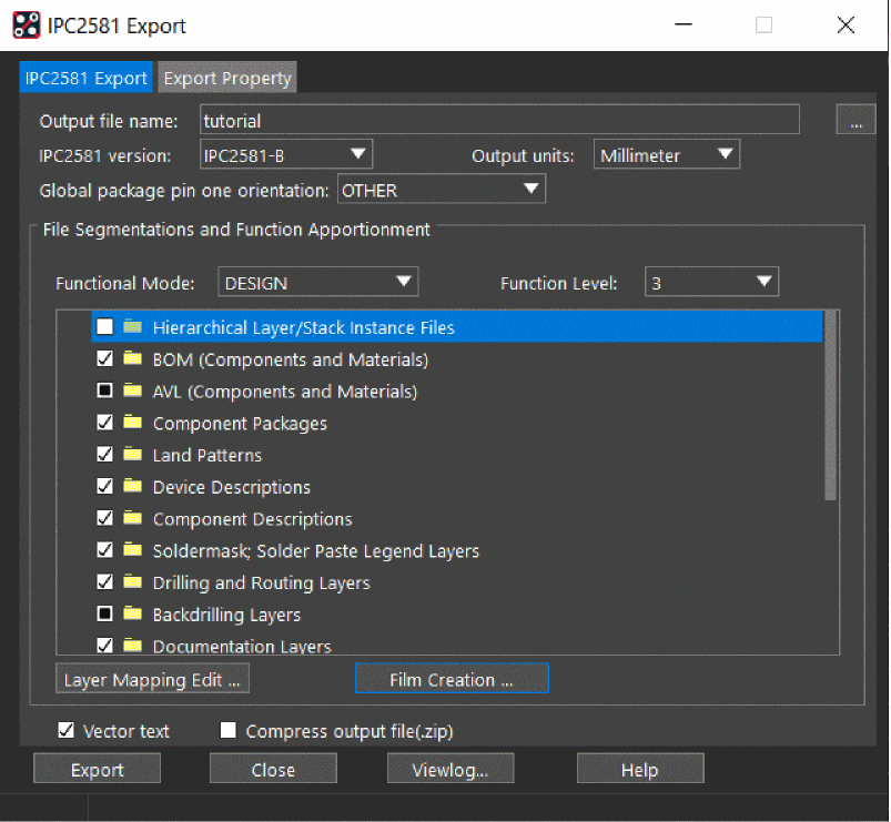
- Leave the IPC2581 version to default, which is set to the latest version IPC2581-B.
- Select Output units to Millimeter.
- Set the Functional Mode to DESIGN and Level to 3.
Five functional modes are supported and each mode consists of three levels that define the complexity and detail of the output file.
Click Film Creation to add class and subclass for film records.
The Artwork Control Form opens. - Select both the TOP and BOTTOM layers and click OK to close the dialog box.
Film record creation settings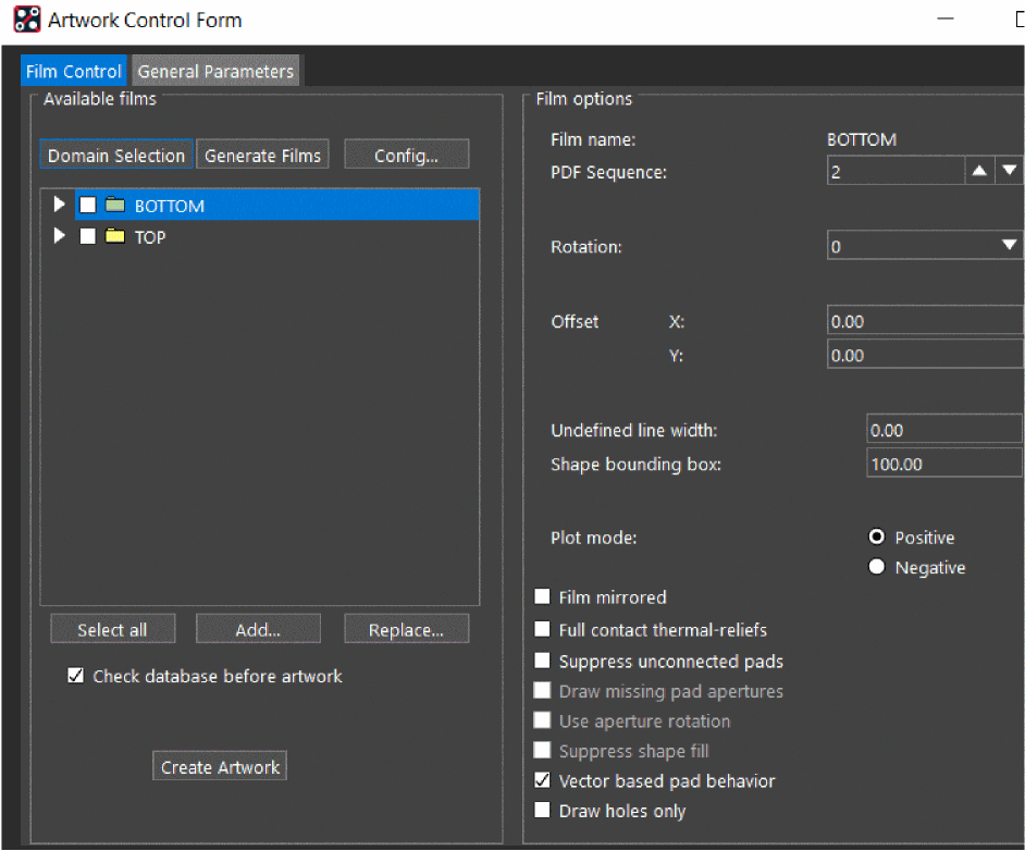
When exporting IPC2581, it is recommended to enable Dynamic unused pads suppression option in Cross-section Editor to suppresses unconnected pads for the selected object types (pin/via) on the selected inner layers.
- Click IPC2581 Layer Mapping Editor to specify layer type for each artwork film.
- Select the check boxes for Soldermask Layers for both the artwork films and click OK to close the dialog box.
IPC2581 Layer Mapping Editor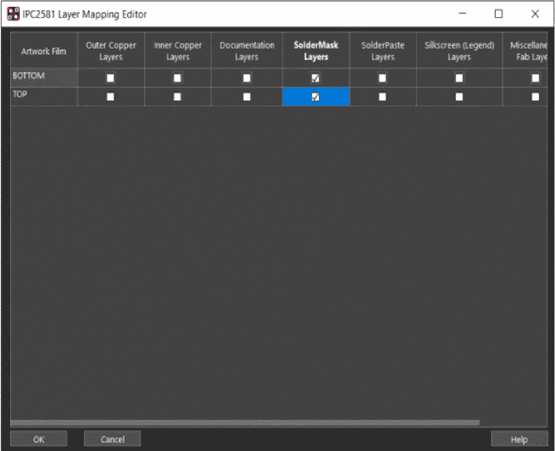
- To generate IPC2581 file, click Export.
An XML file (tutorial.xml) is created in the allegro directory. - Click Viewlog to review the log file.
If you have any questions or comments about the OrCAD X platform, click on the link below.
Contact Us