Solutions For Impossible PCB Designs
If you haven’t already been there, it’s only a matter of time. Every generation of PCB Design becomes more technical than the one that came before. Devices are shrinking while adding more transistor gates. In the same way that the universe is expanding, the silicon is contracting.
Orders of Magnitude Improvements in Electronic Performance
The billions of lightyears we use to measure intergalactic space are a good metaphor for the size and number of our circuits, except in the opposite direction. Just as it is difficult to wrap our minds around the vast distances and age of the universe, so too is the progress on the integrated circuits that power our modern devices.
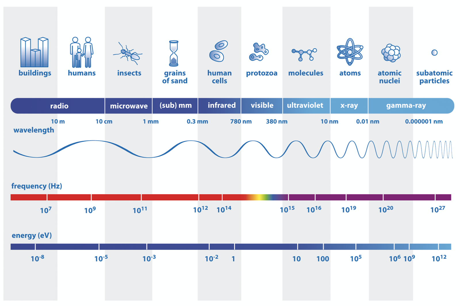
We use the term “nanometers” as if we could see the difference between those and microns. Reality check: a 10 nanometer feature is invisible. When you cut a meter of wire into one billion pieces of equal length, you get down to the proper scale. A billion meters, on the other hand, gets you from Sunnyvale California to the moon and back with two times the diameter of the planet Jupiter left in the batteries. That’s the work of one gigameter. Have you got a minute? Can we talk about 400 Gigabytes per second? A billion is a lot. A billionth is not.
Deeper Than Deep Sub-micron Technology: Can You See Me Now?
Given that the wavelength of the visible spectrum is an order of magnitude longer than the gate size, it’s clear (or unclear!) that no lens in the world can magnify the individual transistors. Visible light waves are between 780 nm and 380 nanometers. Chip makers passed beyond those feature sizes several generations ago.
A 18 nanometer device is advanced while the leading edge is more like 5 nm. The entire transistor gate is larger than that but not by a lot. A scanning electron microscope is required to infer the geometry rather than actually look at it. Supporting circuit density at this level requires new thinking at wafer scale, at chip scale and and at the level of PCB layout.
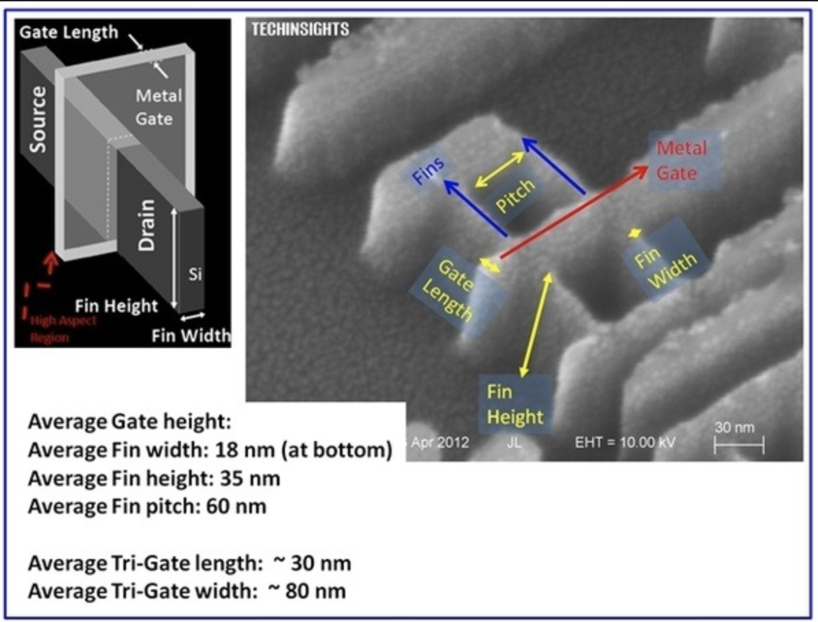
Image Credit: Tech Insights - The road map doesn’t end here, count on it.
Counting by the billion is not just for hardware. The data rates and resonant frequencies moved from “Mega” to “Giga” some time ago. Astonishing performance is expected while failure is not tolerated. How quickly we forget the pause we used to endure before a Youtube video would actually start after clicking play. The little meter barely stayed ahead and often did not so we watched and waited while the sound and pictures came to a halt. Does anyone remember “Buffering”?
That was while we were sitting at home in front of a PC. Now, we have the TV broadcast studio in our pockets and expect it to work flawlessly on the download as well as the upload links. I want my Gigabit WiFi. The infrastructure that supports our appetite for information has a half-life of a few years before it’s obsolete. 5G is in the roll-out stage and 6G is already a topic. There must be some number bigger than either of those two. Work on the pipeline is never done. New chips are smaller, use less power and do more things. How do we support all of that?
Too Many Components, Not Enough Room
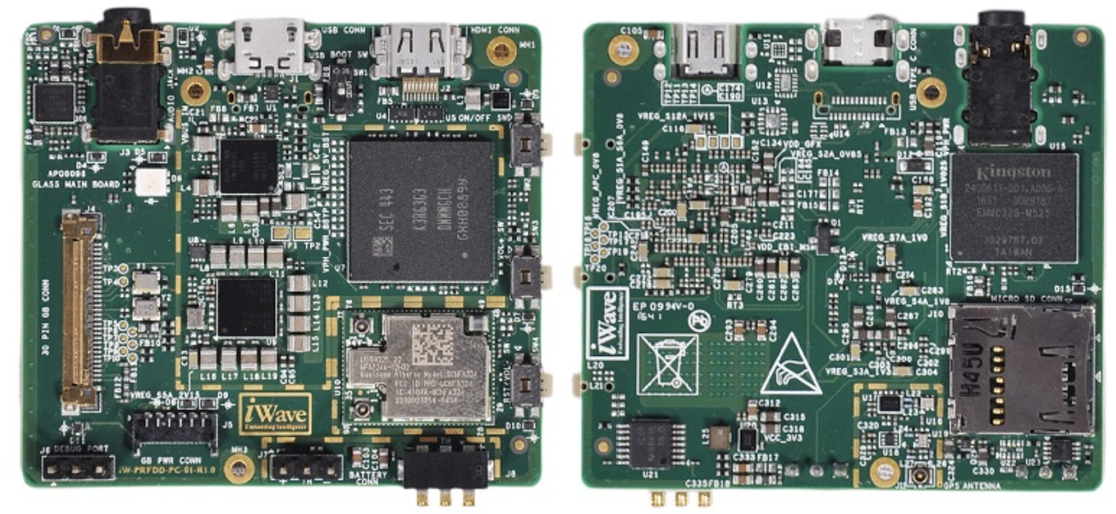
So let’s get to the thick of the plot. Doing all of this magic takes a number of devices. While the microprocessor pulls in many functions that were once handled by separate chips, there are still many more that require their own devices.
Memory chips use a different gate size while analog circuits are not a good fit due to their sensitive nature. Myriad sensors can orbit around the central device. Power supplies come in several types. Some make heat, others make noise. Neither of those things are welcome around the processor cores which make plenty of both on their own.

Image Credit: Author - Maybe it’s not impossible after all but it will certainly take longer to solve.
Power First - Good Voltage Supplies Can Cover For Signal Integrity Sins
Individual power supplies can be combined to form a power management integrated circuit. The PMIC will transform a single voltage into many so that the various “neighborhoods” of the SOC can have a current source tailored to their current draw. Even if they use the same voltage, they are isolated from other domains. It adds up quickly. It is taken for granted that you will get the transmission lines and high speed done correctly. The drama lives in powering up today’s technology with the bare minimum to spare.
The shapes used to connect the PMIC and the SOC are in competition with one another. This is no place for guess work. Simulation is a must-have while sorting out the exact amount of copper for each power domain. Adding to one shape usually means taking from another because we just don’t get unlimited layers. After all of that, we still have to deploy individual power supplies for all of the devices out in the board’s hinterlands.
“...it’s easy to break the equilibrium with even one added via”
The back-and-forth between the Power Integrity software and the layout leads to what I refer to as the border wars. When everything is in balance, there usually isn’t much distance between passing and failing. Everything is close to the margin so it’s easy to break the equilibrium with even one added via cutting through the power planes. Once established it’s best to lock those layers down.
I’m Just an Analog Chip in a Digital World
RF devices are the emo-kids on the block. They do not want to get along with anything else. We keep them shielded in their own little rooms, never to leave the confines of their private Faraday cage. We can force analog siblings to live together but coexistence comes at a price.
At Qualcomm, I was caught in the middle of two chip teams where we had to share a piece of silicon (or was it silicon germanium?) between the WiFi and Bluetooth radios. My buyer pulled me aside and mentioned that it took around 70 board spins of the device under test (DUT) card before we had a working reference board. I was one of three designers and all of us were busy for years supporting that combo chip. Growing the shielded area was never on the table. Impossible is possible; it just takes longer.
Making Sense Out of Sensors
The only thing more emo than radios is the various sensors that are deployed around the board. If you’re ever faced with incorporating any sort of sensor on your PCB, dive into the data sheet and heed all of the advice you can find there. The keep-out area around a sensor is usually much larger than the sensor itself in total area.
This often carries over to all layers below the surface of the board down to the molten center of Planet Earth! Ok, a little hyperbole but not far off. Even the power for the actual sensor is to be considered an aggressor. Neck it down as you get closer to the load pin. Bury it deep within the layers of ground flood. The ground itself is to be especially isolated. It’s a sensor's job to sense things so that’s what they do including any interference that can be detected and amplified. It may sometimes seem irrational but that’s the recipe for success.
Solving “impossible” problems takes collaboration. Shop around for smaller and more efficient components. Take Occam’s razor to the entire schematic. Simulate the signals and the power delivery. Get to know the analog circuits and sensors on an intimate basis. Print that 3dB coupler on an inner layer rather than giving up real estate. Embrace high density interconnect for the space savings and performance gains. Embed some components. Think like a chip maker and improve the circuit in meaningful ways every time it lands on your plate. Go the extra mile to future-proof your designs. Let your imagination run wild. It may seem like a moonshot but remember, we’ve been there and we’ve done that.