Place Replicate - Feature Video
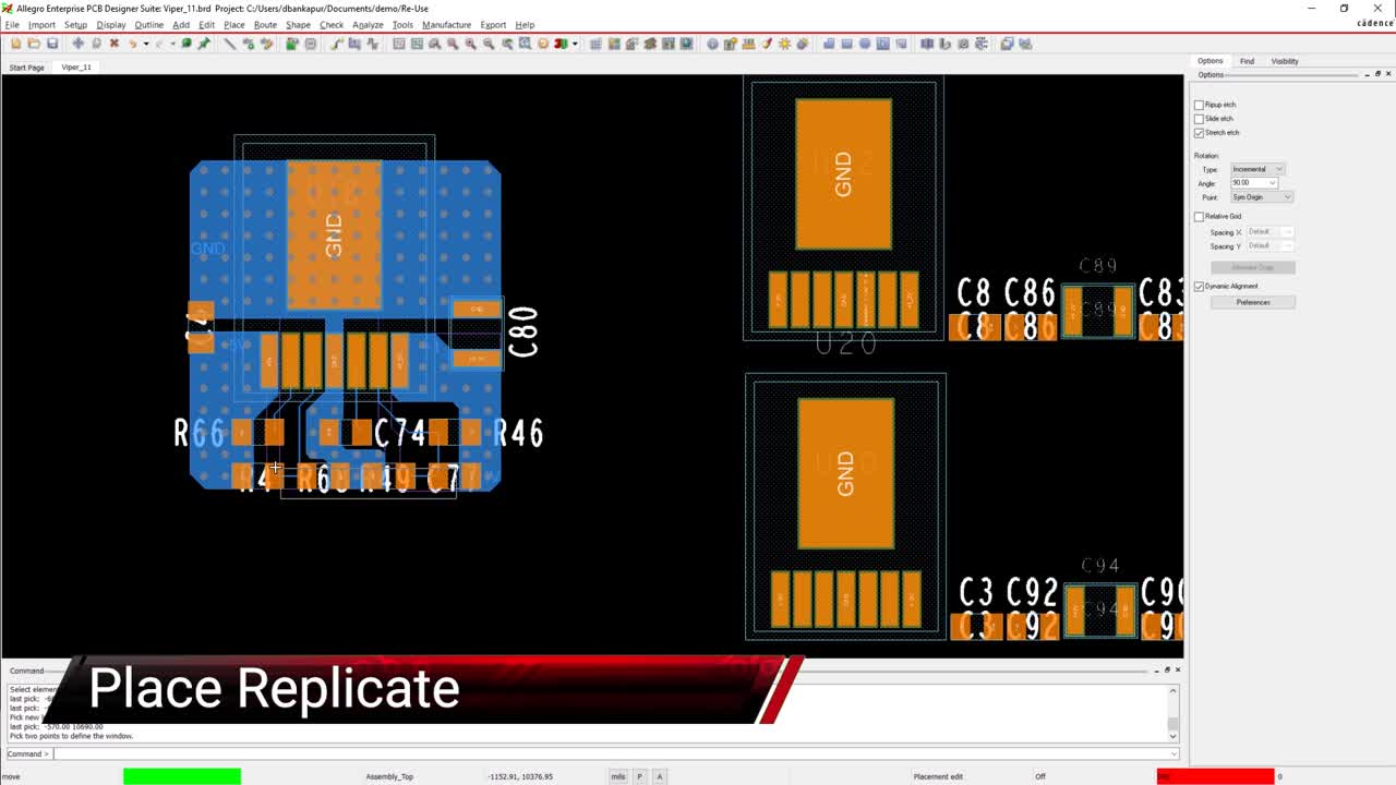
You can create a reuse module from the completed circuitry and save it to your library for future use. Once saved in your library, you can apply the module to the rest of the power supplies in your design. Applying the module is as easy as copy paste in a document, but unlike copy paste, you can manage the module in a library and share it with your whole team.