Home
Free Trial
Home
Free Trial
Read More
Content
Filter
10 results found
Featured
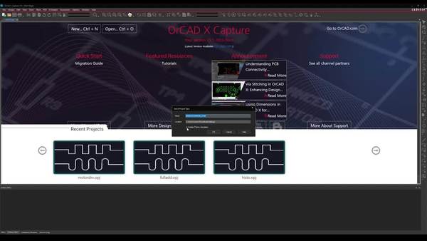
3D CAD Model Library and OrCAD X
Featured
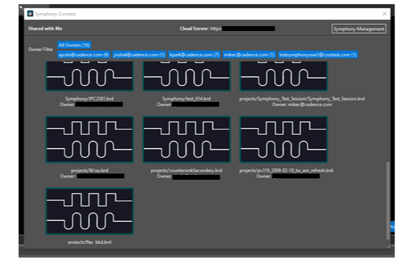
PCB Co-Design Team Spaces in OrCAD X
Featured
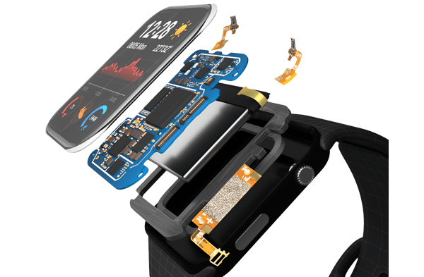
PCB Design for Mechanical Engineers with OrCAD X Tools
Featured
OrCAD X How To - Translating PADS designs into OrCAD X
Featured
OrCAD X How To - Translating Eagle Designs into OrCAD X
Featured
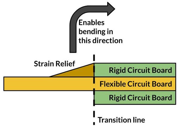
Rigid-Flex PCB Strain Relief Designs: Best Practices With OrCAD X
Featured
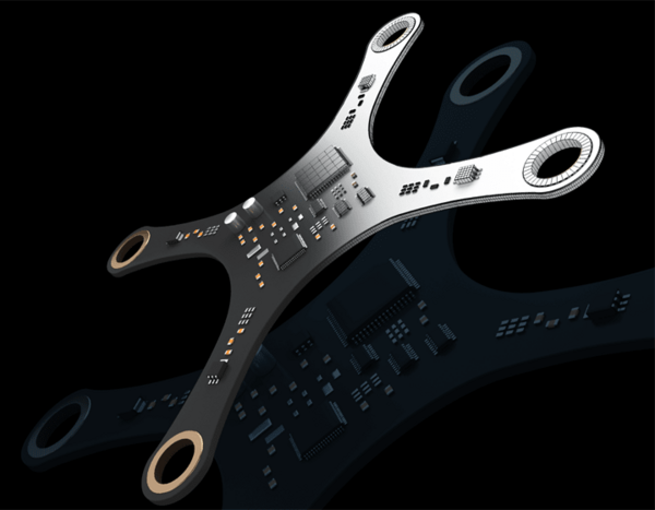
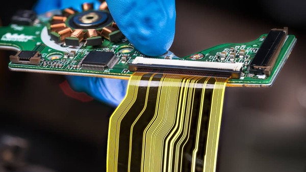
Exploring Flex PCB Current Carrying Capacity
Featured
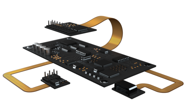
To Design For Rigid/Flex Printed Circuit Boards
Featured
OrCAD X PCB Design Platform Datasheet
Featured
Best High-Speed Routing Practices on Hatched Planes
Featured
Products
None
OrCAD X
(9)
Content types
None
Blog
(7)
Video
(2)
Technical Documents
(1)
Solutions
None
PCB Layout
(7)
Collaboration/Team Design
(2)
Schematic Capture
(3)
BOM Management/Supply Chain
(1)
Constraint Management
(1)
Data & Process Management
(1)
Simulation & Analysis
(2)
Design for Reliability
(1)