The Designer’s Guide to PCB Solder Defects
The Designer’s Guide to PCB Solder Defects
During the inspection process you notice that some passive components aren’t sitting quite right. It seems as though they have pivoted up to stand at attention on one of the two pads that they should be connected to. Unfortunately, a test of the circuit will result in an open.
The resistor stands there like a sentinel, or, aptly, a tombstone to mark the spot of the dead connection. I use the term “resistor” but capacitors and other parts are also candidates. Larger components have the weight to overcome the capillary action of the solder in its liquid state.
Every solder joint goes through its own moment of truth. That moment starts when solder paste reaches a temperature where it acts like a liquid and ends when it freezes into solid metal.

Equal Geometry for Equilibrium in the Oven
Our footprints are typically created with perfect symmetry. The pads are identical and set evenly around the component leads. The pick and place machine, or the human, does a good job of putting the pieces exactly where they go.
Even if the part is not placed exactly right, a well-controlled solder process will have the effect of centering the part between the pads while the solder is in the liquid state. Each pad exerts a capillary force on the lead or ball that it contacts so even if we’re a little off on the placement, our components will self-center themselves under the right conditions. This same capillary action will be the thing that causes the open circuit by lifting the component from one of its pads when the conditions are unfavorable.
That’s where the panic sets in at the assembly house. The assembler has to create the right conditions for 100% of the solder joints going through the SMT line that day and every other day. The PCB design can help or hinder based on a few parameters.
-
Solder volume - How much paste is deposited on the board determined by the stencil design.
-
PCB Thermal Load - Pad geometry and whether copper is flooded or has thermal relief.
-
Solder Paste Composition - This isn’t a board design thing but we are often expected to provide some detailed notes on the assembly drawing.
Adjust the Volume
Most components have a recommended paste stencil opening based and a standard stencil thickness. As the Bill of Materials grows, it becomes more unlikely that all of the vendors assumed the same thickness. If one vendor specified a 4 mil thick stencil and you followed a different component's guideline and used a 3 mil thick paste stencil, it might be necessary to enlarge the paste stencil opening for the component that was based on the thicker stencil. It is kind of hard to know the end-product part-mix when you’re designing the component footprints.
How we use our CAD tool can make or break a soldering profile. If we have an expanded geometry for the solder mask that is larger than the metal definition, then pouring copper over that pad will result in an effective pad that is the size of the solder mask opening. We would call this a mask-defined land. If you were to exert control over individual pads, you could set the expansion to zero where copper is flooded.
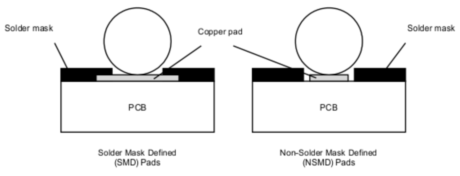
Image credit: All PCB - BGA image but the definition of solder mask types is clear
On the other hand, a non-solder-mask-defined land with a single trace running out would result in a pad the size of the original metal. When the same volume of solder is used for two pads that are different in their effective size it can cause problems. Then add in the fact that pads can act like heat sinks, the differences between the two pads may be too significant for volume production. The factory simply cannot digest that many solder defects and turn a profit.
There are other defects that track with tombstoning such as voids, cold solder, disturbed solder, and, head-on-pillow that occur as a result of imperfect design. While the smallest parts will lift, the larger components may exhibit other defects that have the same or similar root causes. Taken together, the price of rework or warranty repairs and replacements will eat into projected profits for the company.
Warm up the Oven
After the pick-and-place robot has placed all of the parts down into the paste, the board enters the oven for a pre-heat stage that is calibrated to bring everything to a near meltdown before setting off the pulse of heat that finishes the act.
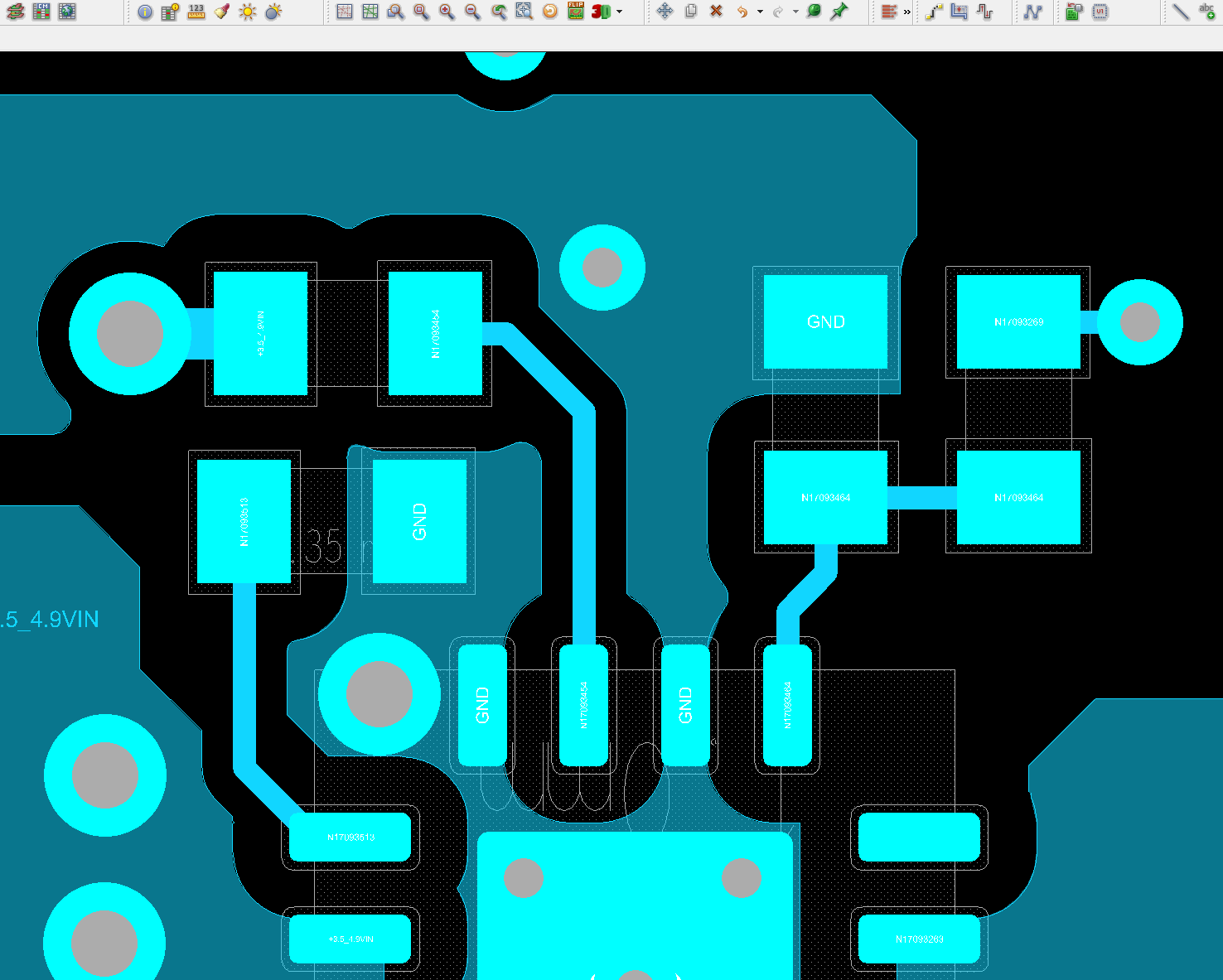
Image credit: Author: notice the unequal copper use on two of the pins
The pre-heat stage will have a uniform effect whenever the effective pad geometry is the same. The non-uniform pads will behave in a predictably non-uniform way. One pad will reach the magic temperature before the other one. The pad that solidifies first will be the one to pull the component up into the tombstone position.

Image credit: Author - now we see the spokes that help equal out the thermal excursions during soldering
Paste it Down
There are a number of variables to solder paste. The particles of metal and the suspension material have characteristics that determine the temperature range of the soldering process and the places where you can sell or dispose of the end product. From start to finish, solder paste is a fluid ingredient to success or lack of it.
The best thing that can be said about a type of paste is that it is eutectic. The meaning of that word is that it liquefies and re-solidifies over a very narrow temperature band. When the solder sets over that small window, there is less of a chance for the junction to be disturbed somehow. It doesn’t take much for the capillary action of the molten solder to pull the part up like a drawbridge.

Image credit: Metal Rescources (pdf) - typical tombstone effect
Flash freezing is awesome. Recreating the properties of the original eutectic solder, a mix of 63% tin and 37% lead has proven difficult. The relatively low melting point of Sn63 solder made it more process friendly. Component makers have to re-engineer their products to withstand reflow temperatures above 200 degrees C in order to use the newer solder pastes.
Formulas with traces of silver and copper are the green choice. Silver isn’t as precious as gold. That doesn’t make it cheap though. The higher temperatures and longer exposure to paste in the vulnerable liquid state increase the odds of components standing on end while being soldered.
About Flux
A definition from the solder makers at Kester:
“A solder paste consists of a homogeneous dispersion of solder alloy powder in a stable viscous flux vehicle. Besides the alloy nature,the metal load, the particle size distribution (or powder type per IPC classification), and the solder paste rheology, the flux chemistry plays a key role to mediate the formation of intermetallic bonding between pads and components.”
The flux provides three benefits:
-
The flux mediates the thermal transfer to the joint area and properly wet the surface
-
It removes the passivation layers and the surface contamination from the PCB pads and component leads
-
It protects the highly reactive molten metals from re-oxidation with the atmosphere until the solder alloy re-solidifies to form the joint during rest of the reflow process.
The flux makes up about half of the volume and 10% of the weight of the paste. For higher reliability, we usually want to clean the flux from the PCB so add that note to your assembly drawing or specify a flux that is not meant to be cleaned. No-clean flux is typically low activity, low residue and free of the harmful ingredients known as halogens. The metals and chemicals in the solder paste are key to good process control.

Image credit: Electronics stack exchange
It’s Library, it’s Placement, it’s Routing, it’s Everything!
Starting with good component footprints and managing the way they are placed and routed is important. This way the solder joints behave in the synchronicity helping you stay out of the graveyard full of tombstones. Similar thermal loads and orientation on the board for each component help reduce the problem.
At the small end of the part sizes, (0201, 01005) a pair of D shaped pads is advisable. Larger components stay down better. Beware of shadows of tall components as they can create cold zones. Keep the components away from the edge of the PCB as it gets hotter faster than the inner areas.
Stay up on your communication with the assembly team whether internal or external. Ask if any particular component is failing in the IR oven. See if there is anything about that part that you can improve. Do this continuous improvement on new products as well as mature ones. It is never too soon or too late to make life easier at the factory.