Home
Free Trial
Home
Free Trial
Read More
Content
Filter
7 results found
Featured
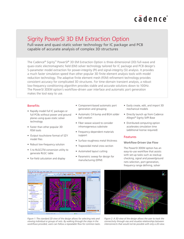
Sigrity PowerSI 3D EM Extraction Option
Featured
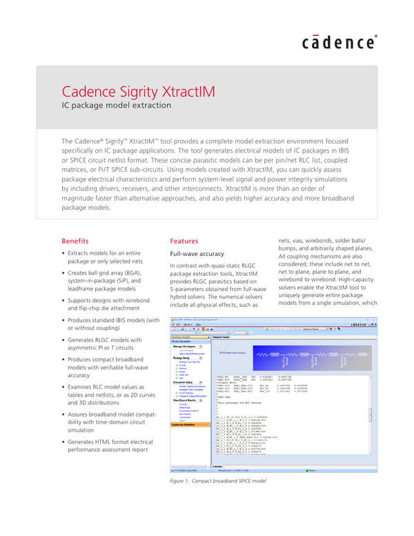
Sigrity Xtractim
Featured
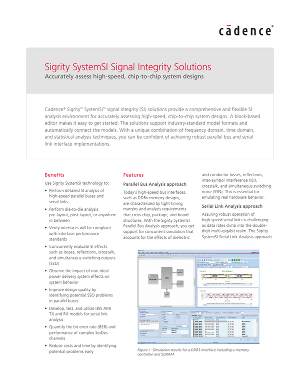
Sigrity SystemSI Technology
Featured
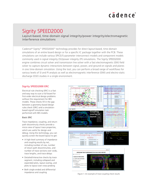
Sigrity Speed2000
Featured
Sigrity PowerSI
Featured
Sigrity PowerDC
Featured
Sigrity OptimizePI
Featured
Products
None
Sigrity X Aurora
(7)
Content types
None
Solutions
None
Design for Reliability
(1)
Thumbnails
Document Outline
Attachments
Layers
Current Outline Item
Previous
Next
Highlight All
Match Case
Match Diacritics
Whole Words
Color
Size
Color
Thickness
Opacity
Presentation Mode
Open
Print
Download
Current View
Go to First Page
Go to Last Page
Rotate Clockwise
Rotate Counterclockwise
Text Selection Tool
Hand Tool
Page Scrolling
Vertical Scrolling
Horizontal Scrolling
Wrapped Scrolling
No Spreads
Odd Spreads
Even Spreads
Document Properties…
Toggle Sidebar
Find
Previous
Next
Presentation Mode
Open
Print
Print
Download
Download
Current View
FreeText Annotation
Ink Annotation
Tools
Zoom Out
Zoom In
Automatic Zoom
Actual Size
Page Fit
Page Width
50%
75%
100%
125%
150%
200%
300%
400%
More Information
Less Information
Close
Enter the password to open this PDF file:
Cancel
OK
File name:
-
File size:
-
Title:
-
Author:
-
Subject:
-
Keywords:
-
Creation Date:
-
Modification Date:
-
Creator:
-
PDF Producer:
-
PDF Version:
-
Page Count:
-
Page Size:
-
Fast Web View:
-
Close
Preparing document for printing…
0%
Cancel