Constraint Usage for Via Management
Key Takeaways
-
How many different vias can you use in a PCB design?
-
The organization problems of using a lot of vias in your design.
-
How Cadence’s constraint management system can organize the use of vias in your PCB design.
Vias in a high-speed printed circuit board design.
I know a lot of people who can’t make it through the day without using a list to keep themselves organized. And in a moment of complete honesty, I’m kind of the same way. Although others may find it amusing, a list is extremely helpful for me to keep track of everything from groceries to be bought to chores to be done. Thankfully, the creators of PCB CAD systems recognize this same need and have provided utilities for the organization of the different data objects in a circuit board design.
At one time, PCB layout only used a minimal amount of shapes and sizes for their trace, pad, and via design objects. Not only did the designs of that time not require many sizes and shapes, but the early photo plotters used in the fabrication of circuit boards didn’t have the capabilities to create them either. As PCB designs became more complex, though, and laser plotters replaced traditional vector plotters, the amount and diversity of the sizes and shapes of these design objects grew exponentially.
Fortunately for the complex PCB layouts of today, designers can rely on constraint usage for via management to help organize the number of objects that they are using in their designs. Like working with a grocery list, these constraint systems can help keep the vias organized and assign them to the nets that they belong to. We’ll take a look here at what some of the problems are that these constraint systems can solve, as well as how to best use these utilities to organize your design.
How Many Different Via Types and Sizes Are Too Many for a PCB Design?
As we originally mentioned, there used to be restrictions on the number of vias that could be used in a PCB design. Not only did designers have to match their trace widths, pad shapes, and via sizes to the available apertures on a photoplotter, but the design tools often didn’t support many different sizes and shapes either. With the current CAD tools and imaging processes being used for PCB fabrication today, however, these limitations are no longer relevant. Depending on what your particular PCB design needs, the sky's the limit for how many different via types and shapes you can use. Here are some of the variations in vias you will be working with:
Via types
There are three main types of vias that are used in PCB designs:
-
Thru-hole vias are the most common as well as the easiest to fabricate. They do have a minimum size limitation, however, and take up a lot of room in high-density designs.
-
Blind and buried vias either start on an external layer and only go partially through the board layer stackup (blind), or only span between internal layers (buried). These vias involve more process steps to fabricate than a standard thru-hole via, but their shorter length is more desirable for signal integrity reasons as well as opening up additional routing channels above and/or below them.
-
Microvias are also known as laser-drilled vias and only span two layers. They are ideal for routing out of dense small-pitch high-pin count components.
Via Sizes
The size of the via can vary quite a bit depending on the hole size that is required. A standard drill usually cannot drill anything smaller than a 0.15mm hole, and anything smaller than that has to be laser drilled in a microvia.
Via drill sizes are also guided by the drill to board thickness aspect ratio, and thicker boards require larger via holes to prevent drill breakage. Usually, the smallest via size permitted on a PCB will be used for signal routing, while larger via sizes will be used for higher current nets, such as power and ground connections.
Via Purposes
There are many different purposes for a via, and the type and size will change depending on what the via is to be used for. For instance, a small thru-hole via is often used for trace routing on a board, while a larger size may be chosen instead for power and ground connections or stitching ground planes together in a gridded pattern.
An even larger sized via can be used for thermal relief underneath components that run too hot to help dissipate the heat through the board. Thru-hole or blind vias can also be marked as PCB test point locations, and some designs may even change the shape of a via marked as a test point from round to square.
As you can see, there are a lot of different sizes and shapes of vias that could be potentially used on a PCB design. The problem now is all of the confusion that can come from trying to manage that many objects in the design.
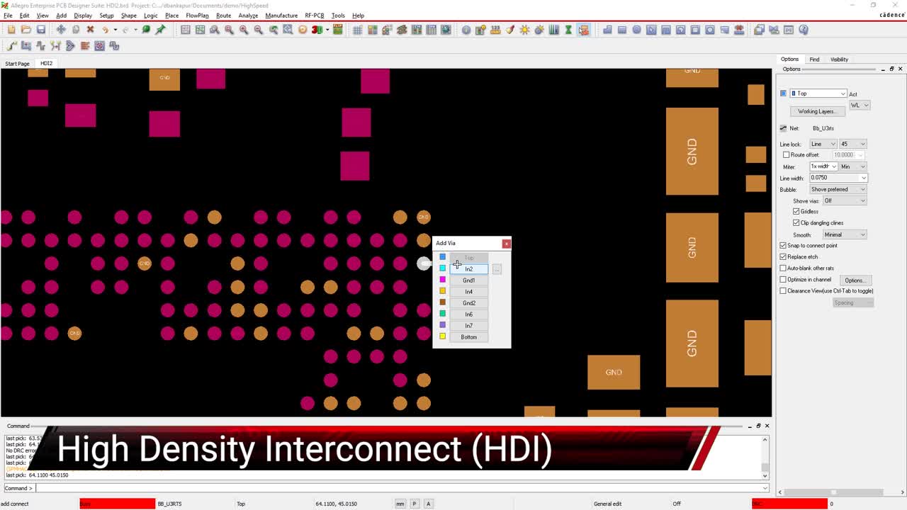
Using the via list capabilities of the PCB design tools to assign multiple vias to a net.
The Organizational Problems With Vias in a PCB Layout
As we have just described, there can be a lot of vias used in a PCB design. The picture above shows a list of the vias that have been made available for use in one net in the CAD system, while the rest of the nets may be using completely different ones. Additionally, there are many other intelligent design objects that must be managed in a PCB design along with the vias increasing the complexity level of the design. Trace widths, routing topologies, and spacing requirements are just a few of those items that the designer must carefully set for use according to what is best for the layout.
To complicate the design even further, there are often requirements associated with certain nets that absolutely have to be maintained in order for the board to perform as expected. For instance, some high-speed nets may be restricted to certain layers, which means that those nets will need a specific blind or buried via to keep them on the desired layers.
While a designer may be able to track a handful of these restrictions in their head and use the appropriate vias for those nets, it gets a lot more difficult when the design has hundreds of these rules to manage. Situations like these are a leading cause of design errors that result in poor performance or outright failure of the circuit board during operation. Thankfully, there are utilities in design tools that can help with the management of the different vias being used on the board and their net assignments.
Using a constraint management system to assign vias to individual nets in a PCB layout.
Constraint Usage for Via Management in a PCB Design
One of the best applications for managing vias and other intelligent design data in a PCB layout is a design constraint management system. Pictured above is the constraint manager used in Cadence’s PCB design tools. These systems feature an advanced spreadsheet-style user interface that allows for easy entry and editing of data in the spreadsheet cells. With the various menus in the spreadsheet, you can also quickly pick specific items, such as vias or net names, from a list instead of typing them in.
Constraint management systems like this allow for the simple creation of rules for items, such as trace widths and spacing on individual nets. You also can combine different nets into groups using net classifications, and then assign rules to those classes as well. In addition to routing, these systems also will allow you to set up electrical, component, and DFM rules that will detect problems that could potentially affect the manufacturability of the board.
Spreadsheet-style constraint systems like this can help you organize your layout and design it so that there aren’t any problems in the layout before you send it out for fabrication and assembly. Next, we’ll look a little closer to see just how the vias are used in a constraint management system like this.
Setting up the vias for a PCB design in Allegro’s Constraint Manager.
Examples of a Design Tool Via Constraint Management System
Using the Constraint Manager in Cadence’s Allegro PCB Editor is a very straightforward operation that can be performed in layout or the schematic if you prefer. As you can see in the picture above, different vias have been added to the nets displayed in the constraint manager.
You can select nets individually to add vias or select multiple nets in the manager at once to add the same vias to all of them. These vias are accessed from the list of vias that are available in the design, which can be either created by the designer or imported from a library. With the vias in place in the net rules, the designer can route knowing that you will be using the correct via for each net of the board.
To learn more about using vias in printed circuit board designs or trace routing in general, take a look at this E-book for more information.
If you’re looking to learn more about how Cadence has the solution for you, talk to us and our team of experts.