PCB Design Strategies For Survivability

PCB Design Strategies For Survivability
Face it; we’re hard on our equipment, especially our favorite gadgets. They get squashed to the point of deformation in our pockets. They get bounced around the floor of our cars and abused in so many unintentional ways. If the screen didn’t crack and the battery didn’t fade, it would last until you needed a new one for technical reasons. All of our stuff should be awesome like that. Not breaking is one of the best features to have. That would be the ideal world. Meanwhile, back here in the real world, we’re resource constrained. When we keep score with money, every buck counts.
“Hardware isn’t easy. One major goof can wipe out or severely diminish the returns on the whole investment. I like it back in that ideal world where warranty costs are a small sliver…”
We simply can’t over-engineer everything, so we spend the balance of our time managing risk. The risk comes in the form of a thousand little cuts to the once beautiful power-plane. Slots for this and vias for that perforate the interior while other shapes edge away at the perimeter in what I’ve come to call, “The Border Wars.” The same walls close in around the high-speed busses as all of the other connections are formed. The best layout probably has everyone at the design review equally concerned but aware of the trade-offs and accepting the workarounds and compromises as they relate to their subject of expertise.
After sweating those details and reacting to the last minute improvements, the game is on. So many parts come together from around the world and land on the first PCB; one of many coming down a conveyor belt. A smaller and slower conveyor belt is set up in anticipation of money going in the other direction; your direction. It is go-time. Boxes go to cartons, cartons to pallets then to trucks and onto ships heading for big box stores near everyone. Products on shelves end up under trees, and the cycle continues. Ideally. Hardware isn’t easy. One major goof can wipe out or severely diminish the returns on the whole investment. I liken it back in that ideal world where warranty costs are a small sliver of the pie chart representing the Cost Of Goods Sold (COGS).
Is Class 3 Required?
Mission Critical hardware will require a Class 3 level of fabrication and assembly. The criteria are cut and dry. Or is it? The litmus test is: wil a failure would have a more-than-likely chance of harming someone. Those Samsung phones looked pretty harmless until they had the hand-grenade bug. Too much battery and not enough board space. Every smartphone ever designed has gone in this direction, or so it seems. It doesn’t have to fit the Webster’s description of mission-critical to benefit from ruggedization. The focus on cleanliness and all of those test coupons set Class 3 apart from the rest.
Can you get reliability out of Class 2?
Answer: You get as much reliability as you design into it. Comprehensive testing is the first step. There will have to be a burn-in process to identify and sort out the infant-mortality that plagues most New Product Introduction (NPI) efforts. Running the devices at 80% of their rated power capacity while at 80% of their upper-temperature limit for three days will get a confession (a failure) out of all but the ready-for-prime-time stuff. To be even crueler, we can run the test while the temperature cycles up and down. Then we can make them power on and off over another arbitrary schedule.
The proving ground moves over to the shaker table where all of the mechanical connections get put to the test. It won’t necessarily yield the enduring functionality of the top grade. It will, however, lower the return rate. That’s a good thing. Another benefit is that you can step into the burn-in room for a few minutes to warm up after a cold ride to work. Just kidding. Stay out of there; torture is for the devices.
One of those “Don’t try this at home” tests is dropping the unboxed unit onto a concrete surface from three feet up. The drop test wrecks good products in the effort to make even better products. Drop it at just the right angle so it breaks. Add stiffeners or gussets or whatever it takes to secure everything, then simulate that configuration and refine the whole enchilada for the next new and improved version.
Some DOs and DON’Ts for Enhanced Survivability.
DO
-
Underfill/encapsulants
-
Elongated Pads (Max Footprint Sizing)
-
Heat Sinks/Clamps
-
Mechanical Fasteners
-
Printed Components
-
Embedded Components
DON’T
-
Sockets
-
Relays
-
Potentiometers
-
The Smallest Packages
-
The Heaviest Packages
Underfill is pretty amazing. Ok, it's pretty much super glue. The amazing part isn’t even the stickiness for which it is well known. The cool app is that it can retard the natural expansion and contraction of the PCB-to-package area due to temperature. The coefficient of thermal expansion differs among the various materials. Generally, the silicon (or other chip material) is more stable than the board. The board fluctuates with the weather and repeated excursions to operating temperature. The thing is, underfill is best when used over small areas. Holding something in suspension against its nature creates a little stress at the boundary.
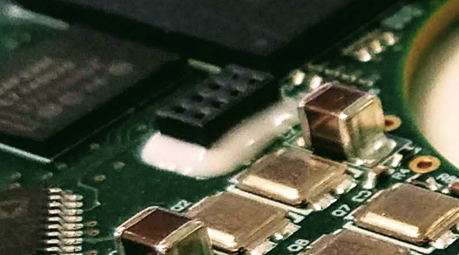
Image credit: Author - definitely not Elmer’s glue, just an insurance policy.
Minimizing the impact of those repeated temperature cycles extends the life of the Ball Grid Array (BGA) type devices. An encapsulant does the same thing but uses an amber-like substance over the electronics that might be found by some civilization millions of years from now. They, will, of course, blame it on ancient aliens.
The Footprint Library Matters
The larger pads serve to increase the personal space of every component that uses them. The additional toe area makes rework less risky. Small pads lift away from the board more easily. The thing is that some lead types, gull-wing for instance, do not want an oversize toe fillet area. The reason is that the bends in the leads relieve those same thermal stresses. A big pad under the inner portion of the lead will allow a larger fillet that negates the springy action of the lead. Soldering, in general, is a fussy process. Solder defects take up page after page of most workmanship manuals.
We want to provide that ideal solution, but again, we have to balance that with performance once the new owner turns it on. When it comes to making someone’s life easier, my first pick is the user, followed by the assembly house, and then the fab shop. The reason I’d push the fab shop over the other two is that they are at the point where our investment is the lowest. Once we factor in the value and time of assembly, I want something boring and repetitive. If we can avoid all of those solder defects on all of those boards, we’re already halfway there.
Let’s Get Some Methodology
All of that shake and bake we do while using the more brittle lead-free solder on smaller and smaller parts, a few solder defects are inevitable. Our main variable besides the metal itself is the amount of paste used. Voids suggest that we want more. Solder balls indicate too much. The oven’s temperature profile can be another of those defect drivers. Our approach to these things in the Board Room is to document as much as necessary and make it better the next time. Printed and embedded components aren’t going anywhere, and they are not getting changed so make sure they are characterized well before cutting them in on the design.
Solid state components with no moving parts are more durable. Membrane switches and other technology mostly eliminate the need for rotary knobs. There are exceptions like electric guitars where the potentiometers should be of the highest quality you can get. Ignore those bean-counters that couldn’t crunch a bar chord anyway. Heavy components are not good at sudden deceleration. With no hardware to keep them snug, they like to rip the pads right off of the board. I know I’ve told that story where we failed the drop test when the USB-C flex circuit wouldn’t stay put.
Widen the process window
Take the continuous improvement approach. Learn from mistakes and try to find some middle ground between the cost of Class 3 and the lower expectations of Class 2. The notes are always “UNLESS OTHERWISE SPECIFIED” so specify otherwise when it makes sense. Go for the Class 2 call-out but raise the game by enlarging the capture pads on your vias so that you don’t have to tolerate the 90-degree break-out that is allowed for Class 2. An eight mil drill requires a 23 mil pad to meet the two-mil annular ring for Class 3 but only an 18 mil pad for Class 2 break-out. Bumping up to a 20 mil pad allows you to prohibit break-out and accept tangency. This way, the entire hole has to live within the pad on every layer. That has to be better at absorbing the shock of daily use without going into NASA territory and cost.