Cross Probing, Intertool Communication, and PCB Design
Part of your PCB design process can be described as bouncing back and forth between the schematic, which visually depicts the components and their connections as symbols in a circuit diagram, and the layout, which depicts the actual physical dimensions and layout of the PCB.
Before the development of electronic design automation (EDA) tools, making a change to a design often involved taking a hardcopy schematic reflecting the change, and then manually making the change to the layout.
For complex designs, this meant spending a great deal of time searching for components in the abstract world of the schematic and matching them to the physical reality shown in the layout—a tedious task for even the most diligent PCB designers.
Fortunately, EDA tools have evolved to help designers and engineers manage the ever-evolving complexity of their designs. In this post, we’re going to take a look at how cross probing and intertool communication (ITC) greatly streamline the PCB design process.
What is cross probing in PCB design?
Cross probing is a form of ITC that allows for seamless bidirectional communication between the schematic editor and PCB layout tool. It’s the technical term for the ability to select a part in your schematic and see the corresponding part in your layout highlighted in an adjacent window.
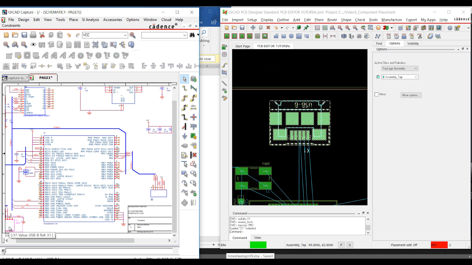
Here selecting a component on a schematic in OrCAD Capture immediately snaps you to a closeup of the same component in the layout in OrCAD PCB Designer. This simple feature saves designers a great deal of time and energy that would have been spent searching for a component.
Advantages of cross probing in PCB design
With cross probing, it’s possible to open your schematic in one window, open your layout in another, and simultaneously select and update different parts in your circuit.
Here are some of the advantages you get with cross probing:
-
Click on pins, pads, buses, components, traces, and nets in one tool and simultaneously locate and highlight them in the other.
-
Use split screen to retain a bird’s eye view of your circuit logic in the schematic as you modify your layout.
-
Take advantage of general ITC to be sure part properties are uniform and up to date across editors.
You can even go into the constraint manager, view a list of component nets, select one and simultaneously see it highlighted in both your schematic and layout. Cross probing has done so much for the EDA workflow that it’s now a seamless part of the experience. It’s hard to imagine life as a PCB designer without it.
Set up your PCB designer toolkit
A field engineer wouldn’t leave their home without all their tools, so why should PCB designers be any different? ITC is much easier when you use tools from the same family of EDA products. Check out Cadence’s suite of PCB design and analysis tools today!