Types of Transmission Lines in High-Speed PCB Layout
Key Takeaways
-
Understanding transmission lines and their different types in high-speed printed circuit boards.
-
PCB transmission line layout techniques.
-
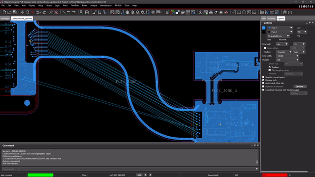
Using your PCB CAD tools to help with the design of transmission lines.

High-Speed PCB routing usually involves transmission line configurations
The demand for the next best thing in electronics continually pushes circuit board technology to higher capabilities and performance levels. To support these enhancements, circuit board designers are working with faster and faster signal speeds every day. At one time, high-speed signals were an occasional design challenge, but now they are becoming a normal part of the design process in PCB layout.
Successful high-speed layout requires designers to understand the principles and techniques of working with high-speed transmission lines on their boards. No longer can traces be routed purely for aesthetics or cost reduction. Instead, the priority is creating the most optimum trace routing for maximum signal performance and eliminating as many signal integrity problems as possible. To do this, designers need to understand the types of transmission lines they will be working with and what layout techniques are best for their design.
Transmission Lines in Printed Circuit Boards
PCB layout designers have routed traces for a long time without worrying about signal integrity issues with the lines. This is because short traces operating at lower frequencies do not create the conditions that cause signal integrity problems. However, higher signal speeds coupled with longer traces will change the behavior of the trace into a transmission line. The delay of the high-speed signal traveling through the line and back is longer than its waveform rise and fall times, creating the potential for signal reflections.
In high-speed design, most long traces should be considered transmission lines. Trying to deduce when a trace stops acting like a simple conductor and starts behaving like a transmission line is not a simple task because there isn’t a set trace length that causes this change. When the signal’s rise time multiplied by its velocity roughly equals the length of the trace, then the trace will be prone to behaving like a transmission line. Wavelength is also sometimes used as criteria for determining a trace's change in behavior, but signal integrity experts don’t always agree on how this should be calculated. With digital signals having frequency components that vary, there isn’t just one wavelength to work with.
The safe bet is that if you are working with a high-speed signal with a defined impedance value, you should always design a transmission line to the impedance requirements and not worry about the length of the trace. The fast rise and fall times of the signal’s wave can create huge problems if the transmission line effects of the trace are ignored. These conditions can lead to reflections, EMI, crosstalk, and a host of other signal integrity issues. Next, we’ll look at what a transmission line is in a circuit board layout.
Traces on a high-speed design being routed over a ground plane layer
Understanding the Types of Transmission Lines in PCBs
Transmission lines in printed circuit board layouts are created using two conductors: a trace for the signal and its return path on a reference plane, which is usually ground. The two conductors are separated by dielectric material, and the usual construction is traces on a signal layer with an adjacent ground plane. Designers determine the width of the trace by carefully calculating the copper weight of the trace with the dielectric material and the depth separating the two conductors. This ensures the line has the same impedance throughout its entire routed length and is referred to as controlled impedance routing.
There are two general categories of transmission lines that are used in the majority of PCB layouts:
- Microstrip: A routed trace with a single adjacent reference plane for its return path is considered a microstrip configuration. Typically, a microstrip configuration is used on exterior layers of the board, but it can also be embedded in an internal layer, as shown in the image below.
- Stripline: When the routed trace is between two reference planes for return paths, it is referred to as a stripline configuration. As you can see below, a stripline offers alternative configurations, such as asymmetric and broadside-coupled, that a microstrip cannot.
A diagram of the different types of transmission lines in a PCB layout
There is another transmission line configuration where instead of a reference plane, an external signal trace has its return path facilitated by two ground traces on either side of it. This configuration requires exact spacing between the traces along the length of the route, but it isn’t commonly used.
Just about any signal in a high-speed design can behave like a transmission line, including data, memory, clocks, controls, and any other nets in the design. The key is how fast the signal speeds are that you are working with. Signals with a rise time of 5 nanoseconds or less put them into the category of high-speed signals. It is also important for designers to realize that signal speeds are not measured by the clock frequency. Just because a component may have a lower clock speed doesn’t mean that it isn’t a high-speed device with very fast rise and fall times. Now, let’s look at some of the techniques required when laying out these different types of transmission lines in high-speed designs.
PCB Transmission Line Layout Techniques
One of the main considerations when routing transmission lines is to control the impedance of the line by using a specific trace width for the line. If the impedance is not matched along the length of the line, it will create signal reflections and potentially disrupt the signal, leading to corruptions of the data being sent. To control this impedance so that the same value is maintained from the source to the load, designers must calculate the physical characteristics of the board to determine the correct trace width.
There are different ways to calculate the trace widths for controlled impedance routing:
- Use one of the many calculators that are available online.
- Most PCB CAD systems now feature impedance calculators in their software to help designers configure the board layer stackup of their designs.
- Leverage the experience of your PCB manufacturer. These people have been building circuit boards for a long time and they understand exactly what you need for a successful design. Many of these manufacturers will also be able to interface with you directly using the IPC-2581 format. For instance, in Cadence’s Allegro PCB Editor, you can use their bi-directional interface to directly communicate with a similarly equipped manufacturer in the IPC-2581 format. This interface allows you to exchange controlled impedance values, board layer stackup configurations, and manufacturing information.
Once your PCB design database is properly configured, it is time to lay out the board. Here are some design recommendations to keep in mind for transmission line routing:
- Don’t route across splits, breaks, or congested areas in the reference plane—it will ruin the return path.
- Keep transmission lines on one layer as much as possible.
- If you must transition between signal layers, use a ground transfer via next to the trace to continue the return path uninterrupted.
- Keep differential signals together and don’t break them up around vias, etc.
Your PCB CAD tools can help you with all of these tasks, and we’ll look at a couple of examples of this next.
Differential pair routing on a printed circuit board
Leveraging the Power of Your PCB CAD Tools for Transmission Line Layout
As we mentioned above, the bi-direction IPC-2581 interface is an invaluable tool for exchanging impedance-controlled calculations and board layer stackup configurations between your CAD system and your manufacturer. However, there are many other features and functionalities in your CAD system that will assist you in designing high-speed transmission lines as well. One of these is using the full capabilities of your design rules and constraints.
Allegro’s Constraint Manager allows you to set up rules for your design, including how the different types of transmission lines are to be routed. You will be able to restrict the layers that specific nets or net groups can route on, designate vias, and control components and other board object spacings. For controlled impedance lines, you will be able to specify unique line widths for nets or net groups, clearances, line lengths, and differential pair configurations. However, these rules and constraints govern more than just routing, they control all aspects of your PCB design. You can set up specific manufacturing requirements for solder mask coverage and component spacing and many different electrical specifications.
Cadence’s tools can make a big difference between success and failure in how you design high-speed printed circuit boards. Additionally, Cadence also provides helpful information such as how to solve common high-speed design issues that can be found in this E-book.
If you’re looking to learn more about how Cadence has the solution for you, talk to our team of experts.