The Best PCB Grounding Techniques in Layout
Key Takeaways
-
PCB grounding techniques; more than simply routing a net.
-
Power and signal integrity tips for PCB layout.
-
Leveraging the power of your PCB design tools.
A circuit board with an external ground plane
Merriam-Webster says that to be “well-grounded” means having a firm foundation. Usually, this phrase is used when talking about someone’s capabilities, such as “the carpenter was well-grounded in the fundamentals of his trade.” Interestingly, when applied to circuit board design, this phrase takes on the double meaning of both a firm foundation and a well-designed ground system for the PCB. In the world of electronics, a good power delivery network depends on a robust ground system to provide a solid foundation for the circuit board.
Modern high-speed electronics require a well-designed ground system to operate at their best performance. Without the proper care in implementing the PCB ground, the circuit board may experience many different problems with noise and electromagnetic interference (EMI). Here are some additional details on PCB grounding techniques that should help with your next circuit board design.
PCB Grounding Techniques—More Than Simply Routing a Net
The ground net in a PCB design can be deceptive in appearance. Yes, there are many connections, but since most designs will have one or more ground planes in their layer stackup, you just add a via to ground, and the work is done. Right? Technically that is correct, but in actuality, there is a lot more that needs to go into your PCB grounding technique to build a good power delivery network.
A circuit board needs a carefully crafted power delivery network (PDN) to provide clean power to all the components in the design. If not, the board may experience different power integrity problems that manifest themselves in the following ways:
- PDN noise that will cause inconsistent voltage levels.
- Circuitry failure due to insufficient voltages.
- PDN generated crosstalk resulting in signal misinterpretation.
- EMI radiating through the board.
Circuit board designers must lay out their PDN for the best power delivery network to avoid these problems.
Grounding Strategy
One of the first decisions will be deciding what the grounding strategy will be. Lower frequency applications will sometimes use a single point or “star” grounding technique, where the different grounds are tied together only at one point on the board. Higher frequency boards will use a multi-ground strategy where all ground connections on the board share the same plane through low impedance connections. The shortened connections of this technique helps to reduce the EMI that can be created at higher frequencies.
Reference Planes
Another important aspect of your PCB grounding technique is how you configure the reference planes. A signal will use the easiest and lowest impedance route available to it for a return path, which ideally will be a ground plane intended for it. PCB designers must configure their layouts with adequate reference planes with clear return paths to prevent signals from wandering around and creating additional noise and interference. We’ll look more into reference planes next as we examine PCB grounding techniques in high-speed designs.
Shielded areas like this make good use of the PCB grounding techniques designed into the board
Power Integrity in High-Speed Design
The first part of setting up the best grounding strategy for your high-speed circuits is to set up the board layer stackup correctly. Obviously, there are fabrication and assembly aspects that must be considered, which is why it is good to work with your manufacturer ahead of starting the layout for the best materials choices. You will want to set up a stripline layer configuration and partition the design appropriately for the different types of circuitry to be laid out.
Next will come component placement. There are many rules for placing high-speed components, including following signal paths and leaving enough room for escape vias and dense bus routing between parts. For grounding specifically, you will want to place bypass caps as close as possible to the power and ground connections and route them to the ground plane with short direct traces and vias. You will also want to ensure that your parts placement does not inadvertently allow trace routing to cross over plane splits (as exemplified in the picture below). You also need to place your parts so as to avoid other areas of circuitry such as analog or power supply partitions.
One of the goals in designing a circuit board is to lay it out in such a way as to have the best signal integrity possible. You’ve already set up the board layer stackup configuration for stripline routing and you must route your impedance-controlled nets between these ground planes. Successful transmission line routing depends on those traces being coupled with a reference ground plane for the more clear and uninterrupted signal return path. The planes will also help shield the high-speed circuits from internal and external sources of EMI, and the ground planes will also help shield any EMI that the high-speed circuits may produce.
Good PCB grounding techniques will also help with power circuits, which we will discuss next.
Split planes in a circuit board can be used for either power or ground nets
Power Supply Layout
Many of the same general rules for high-speed design also apply to how to lay out the power supply circuitry. For instance, short and direct routing is important in these circuits as well. Here are the power supply layout recommendations that you should consider as you design:
- Component placement: Power components need to be close to each other to restrict the amount of noise they may create in their routing. You still need to be mindful of the design for manufacturability rules from your manufacturer, but keep those parts as close together as possible. This will allow you to keep the traces short. Also, make sure to not place your power components in an area of high-speed digital routing. Keep the different areas of circuitry separated from each other.
- Trace routing: The shorter the power supply routing is, the less inductance can build up in the line, helping to reduce the amount of noise created by the circuit. You must also use traces wide enough to handle the current of the circuitry without risking a burn-through of the trace.
- Signal and power integrity: Whenever possible, use a solid plane for your PCB grounding instead of routing it with traces. This will help with both signal and power integrity and thermal management of the higher currents. Also, ensure that the ground plane is large enough to contain all of the components within the power supply circuitry. This will add another layer of protection from EMI problems.
Creating the best PCB grounding techniques in your circuit board design will require a lot of work on your part, but, fortunately, many utilities in PCB design CAD tools can help.
Design rules and constraints, such as in Allegro’s Constraint Manager, can help with PCB grounding
How to Use Your Design Tools
Designing the best PCB grounding techniques into your circuit board’s PDN will require many different trace width and spacing sizes, plus various component clearance rules. Trying to keep track of all of these values can be difficult unless you use your CAD system’s design rules and constraints. In the picture above, you can see how the Constraint Manager in Cadence’s Allegro PCB Editor is being used to set up different design rules for a power net. In the same way, you can use the constraint manager to set up trace width and spacing for ground nets and component to component clearance values for placing parts. Features like these can help you avoid potential problems with power traces that are too narrow or confined spaces that don’t align with the correct creepage and clearance requirements.
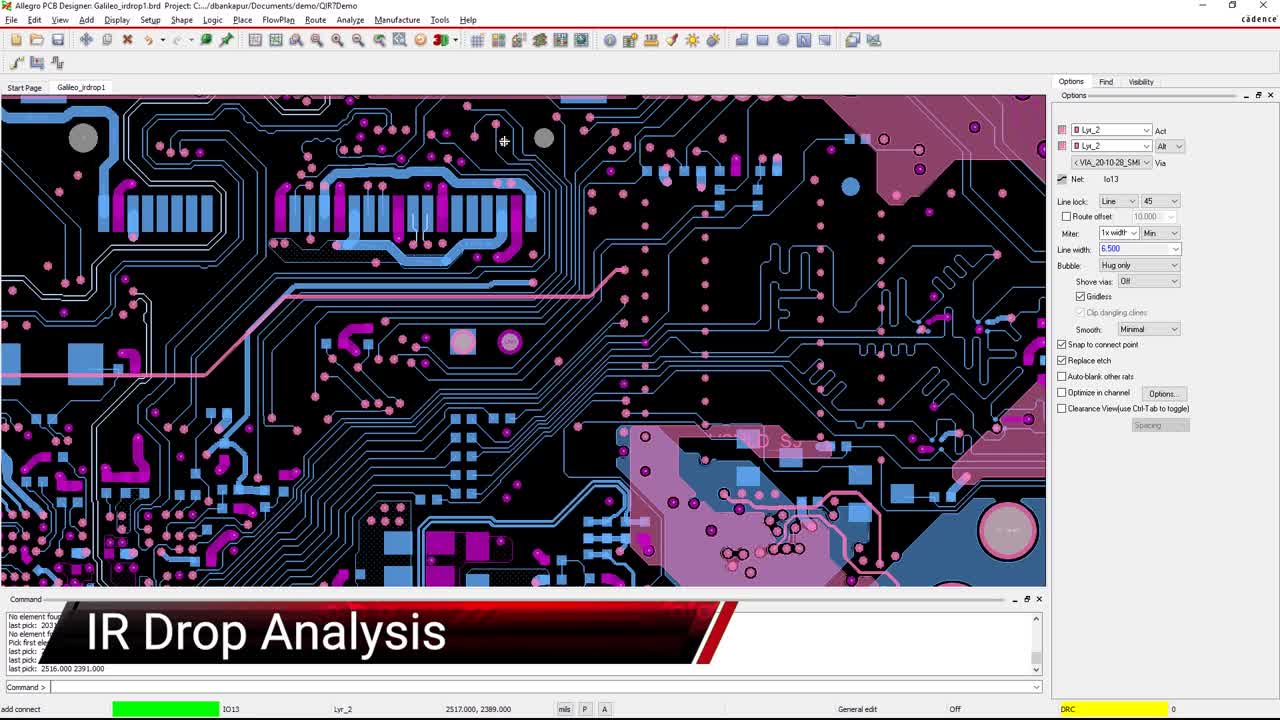
Other useful tools when designing your board’s PDN are the analysis tools that accompany your PCB layout system. For instance, Cadence’s IR Drop Vision can be used directly from the Allegro PCB Editor. This tool gives you a real-time visual display of the power integrity that your design is currently capable of. As an example, it will show you a component pin that needs more voltage from a power net than its routing currently allows for. In Allegro, you can make the correction and then run the check for an immediate verification that the problem has been resolved.
To learn more about working with your circuit board design’s PDN, take a look at this E-book on the subject.
If you’re looking to learn more about how Cadence has the solution for you, talk to our team of experts.