Different Types of Shielding in Analog Layouts to Consider for PCB Design
Key Takeaways
-
Understand potential problems with unshielded electronics.
-
Explore PCB design tactics and guidelines that can help.
-
See how to use metal shields in your next PCB layout.
The classic image of a medieval knight is a metal-clad man armed with a lance or sword and equipped with a shield for defense. In reality, there was much more to the knight’s defense than just his shield. It started first with the knight’s training, included the bulky armor he wore, and was even helped by the young squire who served as his armor-bearer. Although we don’t have much call for the service of a knight today, this same multi-tier approach to defense is still important, especially in PCB design.
Circuit boards can be victimized by incoming electromagnetic interference (EMI) and also affect other electronics with outgoing EMI. There are many solutions to block the interference, including the use of metal shields or cans. The key is to use these different types of shielding in analog layouts, starting first with good PCB layout tactics.
If you’ve been struggling with EMI problems like these, there’s a strong likelihood that the ideas listed below can help.
The Problems That Can Result from Unshielded Electronics
Many types of interference can affect the performance of electronics. These include ground bounce, crosstalk, and power supply noises. The biggest concern, though, is with electromagnetic interference. EMI can have a devastating effect on the normal operation of electronic devices, and the results can be both costly and dangerous. One example is in the medical field where the malfunction of electronic equipment (e.g., monitors, defibrillators, and ventilators) can have grave consequences.
Here are some of the problems that can be experienced by electronic devices if EMI is not properly controlled:
-
Disruption of communications.
-
Interference with wireless devices.
-
Corruption of data from sensors.
-
Electronic component malfunctions.
-
Software errors or failures.
The danger of EMI is twofold: electronics can be victimized by incoming EMI, or a circuit board can generate outgoing EMI that will damage other electronics. There are different standards to govern what is and isn’t acceptable with EMI emissions in order to limit the potential problems. IEC 60601, for instance, sets standards for medical equipment, while CISPR 12 and CISPR 25 cover the disturbances from external and internal sources in vehicles respectively.
The most common source of EMI in printed circuit boards is internal to the board and stems from problems in its layout. If not corrected, the EMI generated by these problems can disrupt the operation of the board to the point where it will ultimately fail. To prevent this, it is important to start with using good PCB design techniques in the layout of the board, which we will look at next.
Short direct routing between analog components.
Analog Shielding Starts with a Good PCB Design
Fortifying electronics against EMI needs to be part of the overall design of the circuit board. Here are the four main areas of PCB layout that should be considered for EMI prevention:
Board Layer Stackup
How the layers are configured in your PCB stackup is an essential first step in the control of EMI. While it may seem attractive to reduce the layer count to reduce manufacturing expenses, that strategy may damage the signal integrity of the board. High-speed signals, sensitive analog nets, and noisy power circuitry all need to be isolated from each other, and that may require additional layers in the stackup. It is also important to provide enough layers for ground planes to shield these signal layers from emitting or being victimized by EMI.
Component Placement
How components are placed will also make a big difference in how the board is shielded against EMI problems. Here are some general guidelines to keep in mind:
-
Keep the analog circuitry separated from the digital circuitry.
-
Keep your analog components placed closely together to keep their trace lengths short.
-
Provide enough bypass capacitors to ensure a clean power delivery network.
-
Include low-pass filtering in your design.
To ensure that your design is EMC compliant, it is important to keep PCB components grouped according to their function. You don’t want digital circuitry to flow through an analog portion of the board, except for those signals that directly connect the two together.
Power and Ground Planes
Metal planes in the board layer stackup provide a lot of shielding, and it is a good practice to route sensitive signals on a layer between two ground plane layers in a stripline configuration. In addition, here are some other guidelines to remember when designing your planes:
-
Use separate planes for analog and digital grounds to keep their noises separate.
-
Provide clear digital signal return paths in the planes that do not flow through areas of analog circuitry.
-
Be careful with split planes, cutouts, or holes in the planes that allow EMI through and can create obstacles for clear signal return paths.
-
Avoid using split planes, but if they are necessary, ensure that the splits only connect to each other at one point. Multiple connection points between split planes can create loops resulting in an antenna that radiates EMI.
Trace Routing
With good component placement, you will already have the foundation necessary for the best trace routing. However, it is still important to follow these routing guidelines to minimize EMI:
-
Keep analog and digital signals separated from each other, and isolate sensitive signals from other routing.
-
Keep analog routing short and make sure that the signals have clear return paths on their reference plane.
-
Use guard traces to prevent crosstalk between two parallel analog traces if you don’t have enough room for the wider spacing. Guard traces also help in shielding between an analog and digital trace, if required.
-
Use vias to form a shielded border or fence between functional partitions of circuitry from each other. Via fences are effective and easy to put in, but the trade-off is that they use up a lot of real estate on the circuit board.
Now that we’ve examined some of the PCB design guidelines that can help with shielding, let’s look at using metal shields on a circuit board.
An analog area of the board protected with a shield.
Considerations for Different Types of Shielding in Analog Layouts
To further shield a circuit board from the effects of EMI, metal shields or cans can be added. The goal is to contain a critical area of the board with shielding that covers all four sides and the top while soldering it down to the ground plane under the components creating a Faraday cage. In a perfect world, the shield would be completely enclosed to block off all emissions. Realistically, however, there needs to be openings in the shield for adjustments, thermal cooling, seams, and solder points to the board.
Another consideration when using shields on a circuit board is that they are usually attached to the board in a manual soldering process after automated PCB assembly. This takes time and adds expense to the manufacturing of the board. It also adds complexity to debug and test, as well as difficulty when reworking the PCB. However, metal shielding does provide a substantial increase in the amount of protection from EMI and is often a requirement for the board. PCB shields can be made out of tin-plated rolled steel, tin-plated copper, stainless steel, and other materials.
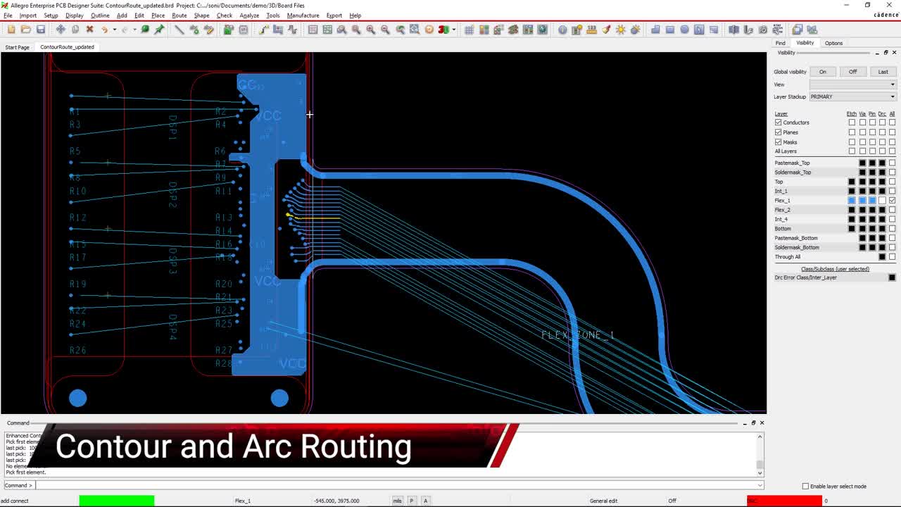
Fortunately, there are PCB design tools in use today that can help with designs incorporating each of these different shielding choices. In the picture above, you can see how Cadence’s Allegro PCB Editor will allow for the addition of a 3D step model of a shield to the design for checking and obstacle clearance. There are other EMI preventative techniques that the tools can help with too, which we will look at below.
Using the Constraint Manager in the Allegro PCB Editor to set up routing rules.
How Your PCB Design Tools Can Help
As we have discussed, the first step of shielding against EMI in analog circuitry is by using good PCB design guidelines. Circuit board layout systems today, like Allegro PCB Editor, have many utilities and features within them to help you stay on track with these guidelines.
In the picture above you can see an example of a constraint management system in Allegro that is used to define net and component classes as well as to set component clearances, vias, trace widths, and spaces. The rules are configured in an easy to use spreadsheet application that allows a wide range of editing capabilities and lends itself well to setting up high-speed design constraints and topologies. The constraint manager will also allow you to set up clearances for many other design objects on the board, including silkscreen and manufacturing rules.
Allegro is a complete PCB design solution that offers its users many different capabilities that will help in designing circuit boards that are protected against EMI. To find out more about EMI control and high-speed design topics in PCB design, take a look at this E-book.
Leading electronics providers rely on Cadence products to optimize power, space, and energy needs for a wide variety of market applications. To learn more about our innovative solutions, subscribe to our newsletter or our YouTube channel.