Design Reuse Within a PCB Layout and Beyond
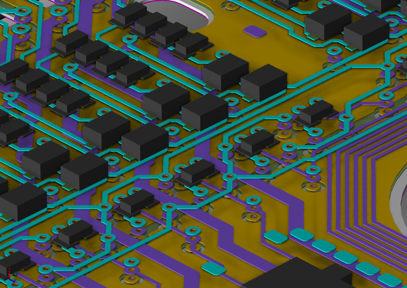
Image Credit: Author - starting small
As PCB Designers, we are often tasked with filling out a board with geometry that repeats itself. Better physical resemblance usually equals better performance. For instance, Ethernet ports will have a transformer right after the connector. They will generally work the same if they look the same. And life will be much easier if you were not reinventing every instance of a circuit. Let’s walk through the process.
Some form of the Copy and Paste commands are always included with our tools. The tools themselves are referred to as PCB editors. The parts we place in the early stages of the design often incorporate parallel paths. Perhaps, all of those identical blocks of schematic diagrams can be randomly placed. Perhaps, not. When I scroll down to the next page and it’s the same as the last page, I keep on scrolling. The schematic may have more to tell.
There are a few intersecting considerations here.
-
Number of Copies
-
Circuit Complexity
-
Timing/impedance Rules
-
Real Estate - or lack of.
-
Future Proofing
Two of a kind with a simple design and ample room is a case where you can do both layouts on a grid and position the groups as required. As the number of copies or the complexity increases, a more formal approach will be necessary. Step and repeat whenever an analog circuit is in play. Multiple Input, Multiple Output (MIMO) is a common architecture that will become even more common with the 5G rollout.
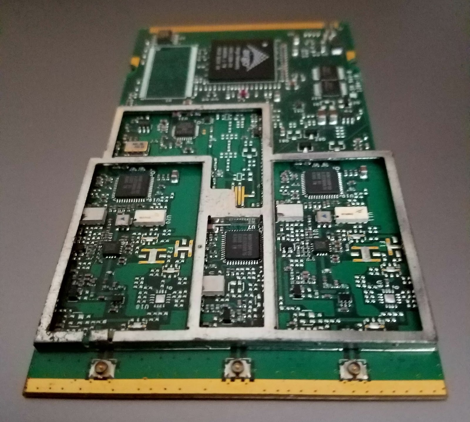
Image credit: Author - MIMO with two RX/TX chains plus one RX.
Go Big
Some advice if you’re moving up to bigger boards: At the very start of a design, the only components that are set within the board outline are those who have a designated location. The most significant device of all is the first one you encounter on a typical schematic. The “brain” may be a simple controller or a System In Package. The central nervous system flows from there. Beyond that, I find it most useful to gather the other pieces into functional groups for a rough placement outside the perimeter. Bear in mind that any of those groups have the potential for reuse.
The unconnected lines and especially the voltage pins will drive a lot of the functional placement sorting. Basically, the components that would suffer the most from being away from the center would get to be near the main device. Bypass caps generally go on the opposite side and everything else crowds around the boss chip.
The Memories
Memory devices typically get the first priority along the processor edges where those pins are located. The evergreen requirement for more memory often relies on using the same device multiple times. The group of components that accompany the repeated memory chips should be as consistently implemented as possible. The routing, while not identical, should be of similar geometry for the controlled-length and controlled-impedance connections.
Note that not that all of the stakeholders have a stake in being close to the main logic device. GPS and NFC devices are likely candidates for the far reaches of the board. Sensors of most types like their open space as well. These are not so much repeated circuits as they are types of circuits with similar functions. The common theme, in this case, is that the devices have trouble coping with noisy neighbors.
When a Copy is Not a True Copy
Repeating a circuit is not always about making exact copies. One instance may be a mirror image of another. Some small attribute might be the only difference among a group of circuits. Resorting to CAD neutral files for these transformations might be the only way out. That really depends on the capabilities of the system. Developing your own creative workarounds for where your PCB layout software is lacking builds character. Going through the deep menus of a fully featured CAD tool will reveal more capabilities than most of us would think of using.
Image credit: Author - mirrored and copied circuits.
Board to Board Reuse
The idea of design reuse from one board to a second one adds another dimension. This is a case where you may not want to be bound to “intelligent” data. Intelligence seems to get lost when there are new circumstances. Reference designators and net names are two attributes that may not carry over to a new design. Stack-Up technology may not be compatible. A clean transfer may mean finding a method that strips away the logic and leaves the geometry to be fleshed out with net and component information.
After a snip of circuitry is imported, it is well worthwhile to fully flesh out the data as much as possible before making any more copies. I did everything perfectly except the silkscreen. Then I turned on the silkscreen layer and got to do that part again and again. Optimize to the bone before creating further instances from that seed. Multiplying mistakes tends to defeat the purpose of design reuse.
Common Clay
Some circuits will be common enough to want to insert into many boards. Voltage regulators are good candidates for saving because they are used everywhere and have special layout considerations. A device like a GPS chip is usually packaged inside of a shield. The shield is usually designed around the circuit and made as compact as possible. Having the shield and the circuit as a unified element makes life easier down the road.
Making copies of subcircuits and archiving them for reuse modules can improve quality, consistency and time to market. As a risk management strategy, using known good designs paves the way to a successful new product introduction. Product families that share some DNA are easier to debug and upgrade when the time comes.
Doing the same job over and over is both boring and a waste of resources. Go ahead and be the one to start a museum of beautiful chip layouts. Reference designs are a leg-up that can help others get up to speed as well. Named for the main device, they can be recalled into action every time they are needed. Save a sub-section, save time, save money, be a hero!